Semiconductor module including a terminal embedded in casing wall and bent over thick portion of lid
a technology of simiconductor modules and terminals, which is applied in the direction of semiconductor devices, semiconductor/solid-state device details, electrical apparatus, etc., can solve the problems of restricting manufacturing costs, and achieve the effect of relaxing the restriction on the length of the bol
- Summary
- Abstract
- Description
- Claims
- Application Information
AI Technical Summary
Benefits of technology
Problems solved by technology
Method used
Image

Examples
embodiment example 1
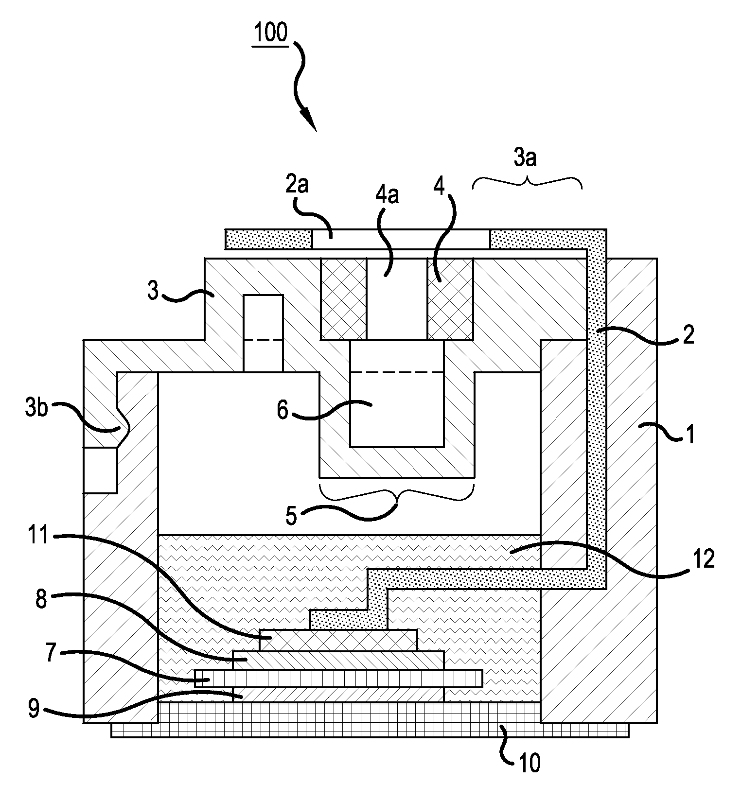
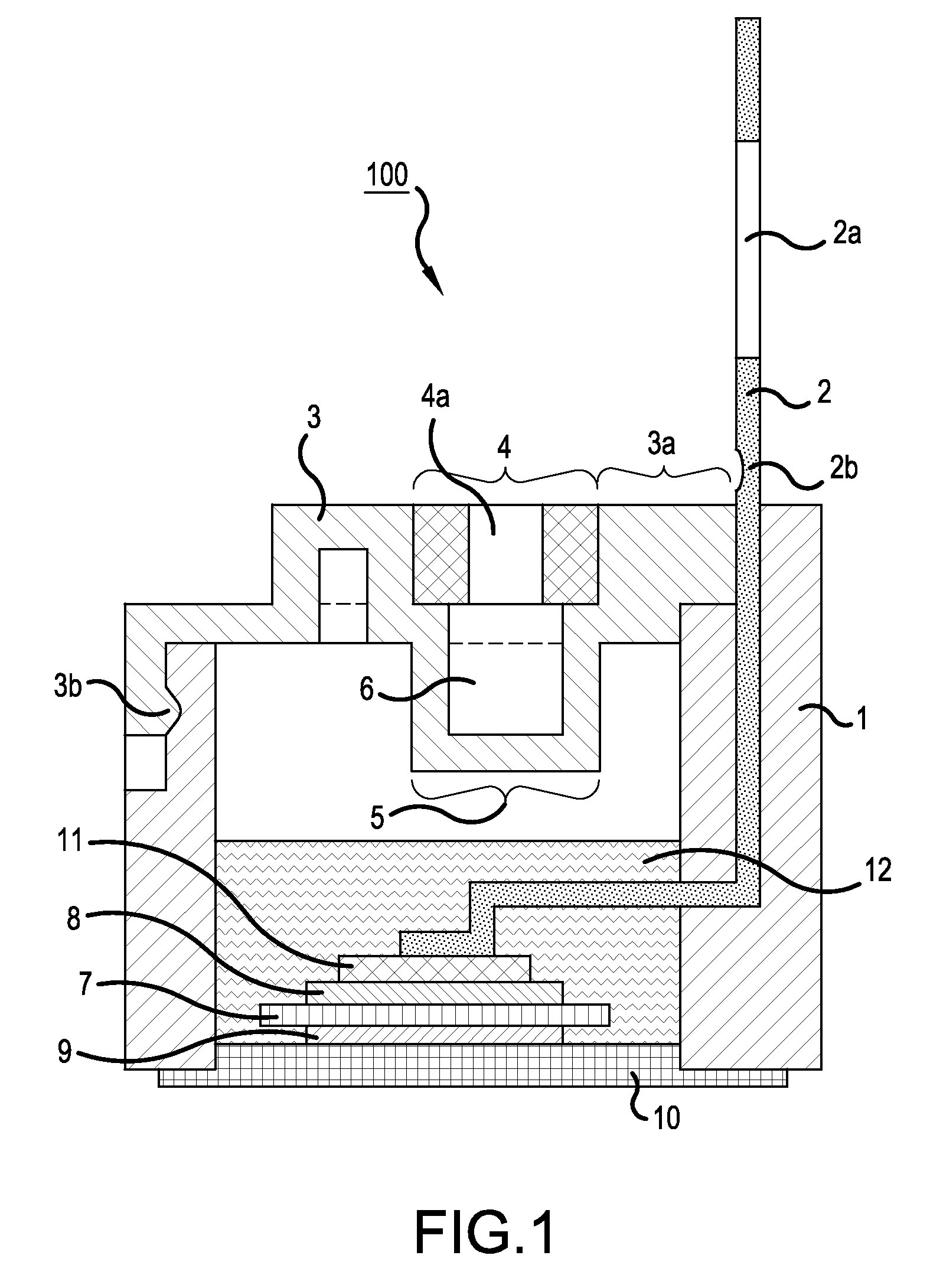
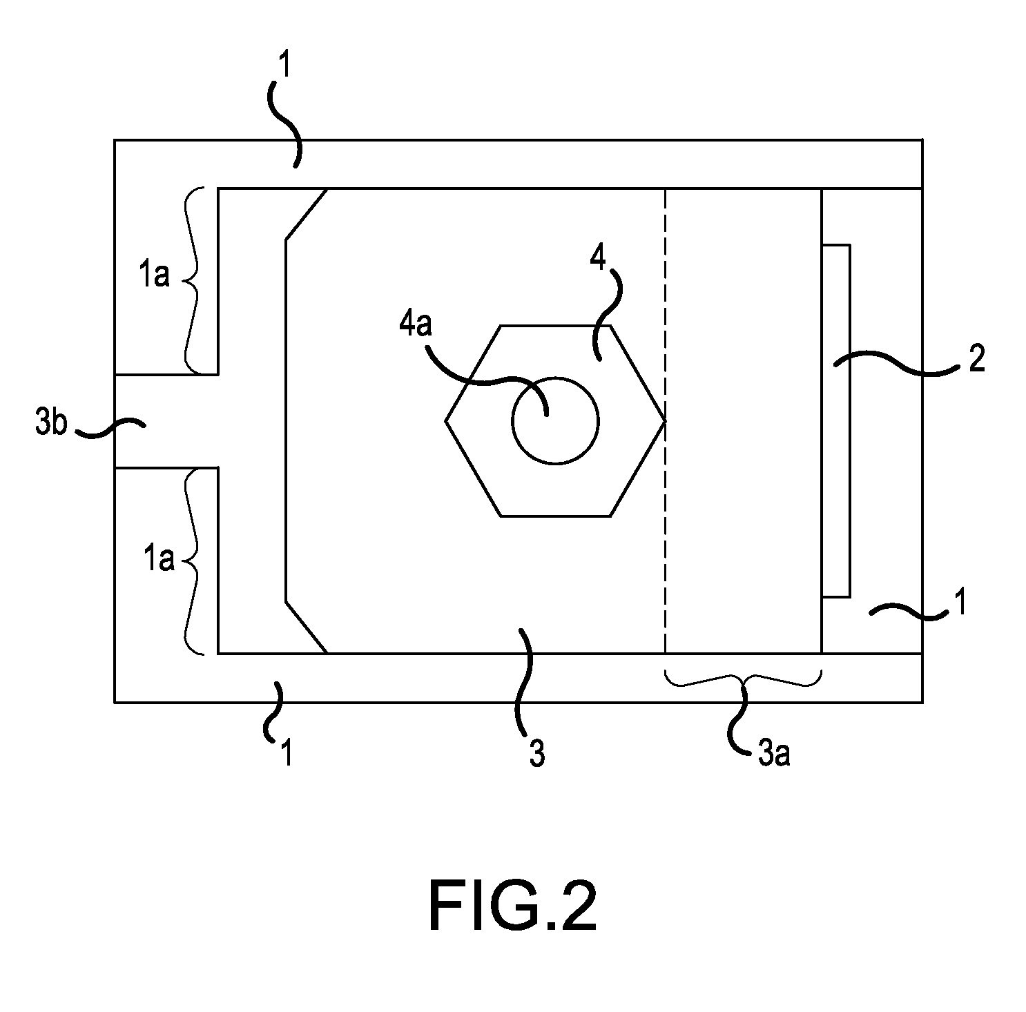
[0038]A first embodiment of the invention, Embodiment Example 1, will be described in the following. FIG. 1 is a sectional view cut along the line A-A in FIG. 3 of a semiconductor module before bending a terminal thereof, according to the first embodiment of the present invention. FIG. 2 is a plan view of a semiconductor module according to the first embodiment of the present invention; FIG. 3 is a side view of a semiconductor module according to the first embodiment of the present invention; FIG. 4 is a sectional view cut along the line B-B in FIG. 6 of a semiconductor module after bending a terminal thereof, according to the first embodiment of the present invention; FIG. 5 is a plan view of a semiconductor module after bending a terminal thereof according to the first embodiment of the present invention; and FIG. 6 is a side view of a semiconductor module after bending a terminal thereof according to the first embodiment of the present invention.
[0039]Referring to FIG. 1, the sem...
embodiment example 2
[0046]The following describes Embodiment Example 2 of the invention. FIG. 7 is a plan view of a semiconductor module after bending the terminal thereof according to Embodiment Example 2 of the invention. This semiconductor module 200 is composed of a plurality of the semiconductor modules according to Embodiment Example 1 arranged laterally. The semiconductor module 200 especially comprises a plurality of terminals 2 electrically connected to different parts of the semiconductor chip 11, the terminals 2 being bent in the same direction. More specifically, the terminals 2 are connected to a gate electrode, an emitter electrode, and a collector electrode of a single semiconductor chip, which can be an insulated gate bipolar transistor (IGBT). Other constructions are same as those in the semiconductor module according to Embodiment Example 1 and details thereon are omitted here.
[0047]Because the lids 3 are provided separately, exchange of only one lid 3 that needs to be exchanged is po...
embodiment example 3
[0048]The following describes Embodiment Example 3 of the invention. FIG. 8 is a plan view of a semiconductor module after bending the terminal thereof according to Embodiment Example 3 of the invention. This semiconductor module 300 is same as the semiconductor module 200 according to Embodiment Example 2 except that the lids 3 of the semiconductor 200 are made monolithic forming a lid 13 and the casing 1 is formed so as to engage with the lid 13. Second engaging parts 13b are provided at the ends of the lid 3 at the opposite side to the thick parts 3a. The second engaging parts 13b works together with the first engaging parts 1a to fix the lid 13 to the casing 1. The side wall of the casing 1 is put between the part of the lid 13 opposing to the first engaging parts 1a and the second engaging parts 13b and fixed. Because the lid 13 is a common lid for every terminal 2, attaching work for the lid 13 is simplified in the assembling process of the semiconductor module 300.
[0049]As de...
PUM
 Abstract
Description
Claims
Application Information
 - R&D
- Intellectual Property
- Life Sciences
- Materials
- Tech Scout
- Unparalleled Data Quality
- Higher Quality Content
- 60% Fewer Hallucinations
Browse by: Latest US Patents, China's latest patents, Technical Efficacy Thesaurus, Application Domain, Technology Topic, Popular Technical Reports.
© 2025 PatSnap. All rights reserved.Legal|Privacy policy|Modern Slavery Act Transparency Statement|Sitemap|About US| Contact US: help@patsnap.com