Apparatus and methods for spacer deposition and selective removal in an advanced patterning process

a technology of selective removal and spacer deposition, applied in the direction of electrical equipment, basic electric elements, semiconductor/solid-state device manufacturing, etc., can solve the problems of light beam out-of-focus issues, overlay errors, and additional processing capabilities, and achieve good profile control

Active Publication Date: 2016-11-01
APPLIED MATERIALS INC
View PDF12 Cites 19 Cited by
  • Summary
  • Abstract
  • Description
  • Claims
  • Application Information

AI Technical Summary

Benefits of technology

[0009]Embodiments herein provide apparatus and methods for forming a spacer layer and in-situ performing a selective removal process on the spacer layer with good profile control in multiple patterning processes to form nanowires for semiconductor applications. In one embodiment, a method for depositing and patterning a spacer layer during a multiple patterning process includes conformally forming a spacer layer on an outer surface of a patterned structure disposed on a substrate, wherein the patterned structure has a first group of openings defined therebetween, selectively treating a first portion of the spacer layer formed on the substrate without treating a second portion of the spacer layer, and selectively removing the treated first portion of the spacer layer.

Problems solved by technology

However, with the continued miniaturization of circuit technology, the dimensions of the size and pitch of circuit features, such as interconnects, have placed additional demands on processing capabilities.
Inaccurate critical dimension or profile deformation of the patterned structure may cause a light beam out-of focus issues, overlay errors and a significant resolution loss during the subsequent lithography exposure process.
In some cases, inaccurate profile or structural dimensions may result in collapse of the device structure, eventually leading to device failure and product low yield.

Method used


Image

  • Apparatus and methods for spacer deposition and selective removal in an advanced patterning process
  • Apparatus and methods for spacer deposition and selective removal in an advanced patterning process
  • Apparatus and methods for spacer deposition and selective removal in an advanced patterning process

Examples


Embodiment Construction

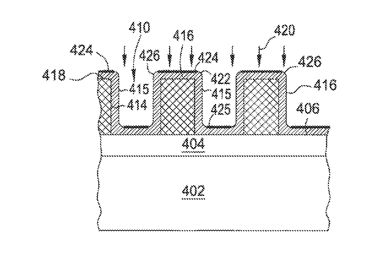
[0019]Embodiments for the present application includes a process to deposit and pattern a spacer layer utilized in a multi-patterning process which may provide a patterned spacer layer with desired accurate dimension and profile without rounded, deformed or eroded corners and / or shoulders. The spacer layer may be utilized in a multiple patterning process which may be ultimately used to pattern and etch a dielectric interconnect material for the formation of metal containing features (e.g., nano wires) with high aspect ratios and / or with small dimensions. In one embodiment, the spacer layer deposition and patterning process may include a deposition process that forms a spacer layer followed by a selective removal process to efficiently shape and control the resultant profile to provide a spacer layer with desired profile and dimension. The deposition and selective removal process may be performed by utilizing an inductive couple plasma source (ICP) deposition process and then followe...


PUM


Abstract

Embodiments herein provide apparatus and methods for performing a deposition and a patterning process on a spacer layer with good profile control in multiple patterning processes. In one embodiment, a method for depositing and patterning a spacer layer during a multiple patterning process includes conformally forming a spacer layer on an outer surface of a patterned structure disposed on a substrate, wherein the patterned structure has a first group of openings defined therebetween, selectively treating a first portion of the spacer layer formed on the substrate without treating a second portion of the spacer layer, and selectively removing the treated first portion of the spacer layer.

Description

BACKGROUND OF THE DISCLOSURE[0001]1. Field[0002]The embodiments herein generally relate to an apparatus and a fabrication process for forming a spacer layer for use in a lithographic multi-patterning fabrication process.[0003]2. Description of the Background Art[0004]Reliably producing submicron and smaller features is one of the key requirements of very large scale integration (VLSI) and ultra large scale integration (ULSI) of semiconductor devices. However, with the continued miniaturization of circuit technology, the dimensions of the size and pitch of circuit features, such as interconnects, have placed additional demands on processing capabilities. The multilevel interconnects that lie at the heart of this technology require precise imaging and placement of high aspect ratio features, such as vias and other interconnects. Reliable formation of these interconnects is critical to further increases in device and interconnect density. Additionally, forming sub-micron size features ...

Claims


Application Information

Patent Timeline
Patent Type & Authority Patents(United States)
IPC IPC(8): H01L21/302H01L21/033H01L21/311
CPCH01L21/0338H01L21/0332H01L21/0335H01L21/0337H01L21/311H01L21/0274H01L21/3213H01L21/76816
Inventor ZHOU, JIEYING, CHENTSAUROY, SHAMBHU N.NEMANI, SRINIVAS D.LIU, JINGJINGYIEH, ELLIE Y.
Owner APPLIED MATERIALS INC
Why Eureka
Try Eureka