Tin oxide and tin carbide materials for semiconductor patterning applications

a technology of tin carbide and semiconductor, applied in semiconductor/solid-state device manufacturing, basic electric elements, electric devices, etc., can solve the problems of high aspect ratio, high processing capacity, and high processing capacity, and achieve good profile control and high selectivity. the effect of patterning process

Pending Publication Date: 2022-06-16
APPLIED MATERIALS INC
View PDF0 Cites 0 Cited by
  • Summary
  • Abstract
  • Description
  • Claims
  • Application Information

AI Technical Summary

Benefits of technology

[0002]Implementations described herein generally relate to a film stack and an etching process for etching the film stack with high selectivity and good profile control to patterning processes.

Problems solved by technology

However, with the continued miniaturization of circuit technology, the dimensions of the size and pitch of circuit features, such as interconnects, have placed additional demands on processing capabilities.
Developing a film stack and etch processes that are capable of reliably forming features with such high aspect ratios presents a significant challenge.
Inaccurate control or low resolution of the lithography exposure and developing process may lead to poor critical dimension of the various layers utilized to transfer features into a film stack, resulting in unacceptable line width roughness (LWR).
Large line width roughness (LWR) and undesired wiggling profile can cause inaccurate feature transfer to the film stack, thus, eventually leading to device failure and yield loss.
Furthermore, during etching of such film stacks, redeposition or build-up of byproducts or other materials generated during the etching process can accumulate on the top and / or sidewalls of the features being etched, thus undesirably blocking the opening of the feature being formed in the material layer.
Furthermore, as the opening of the etched features are narrowed and / or sealed by the accumulated redeposition of material, the reactive etchants are prevented from reaching the lower surface of the features, thus limiting the aspect ratio that may be obtained.
Additionally, the redeposition material or build-up of byproducts can randomly and / or irregularly adhere to the top surface and / or sidewalls of the features being etched, the resulting irregular profile and growth of the redeposition material can alter the flow path of the reactive etchants resulting in bowing or twisting profiles of the features formed in the material layer.
Inaccurate profile or structural dimensions can result in collapse of the device structure, eventually leading to device failure and low product yield.
In addition, poor etch selectivity to the materials included in the film stack can undesirably result in inaccurate profile control, thus eventually leading to device failure.

Method used


Image

  • Tin oxide and tin carbide materials for semiconductor patterning applications
  • Tin oxide and tin carbide materials for semiconductor patterning applications
  • Tin oxide and tin carbide materials for semiconductor patterning applications

Examples


Embodiment Construction

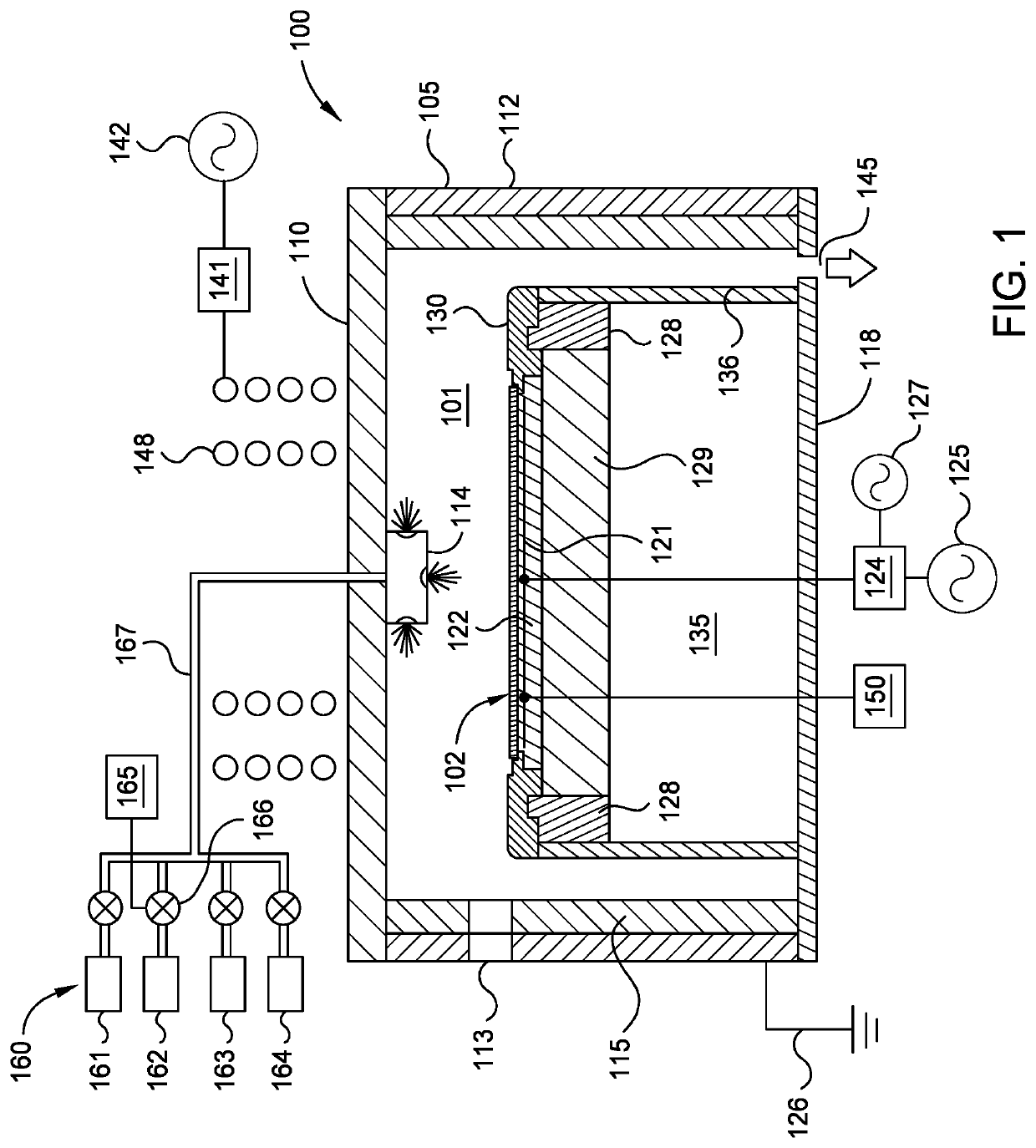
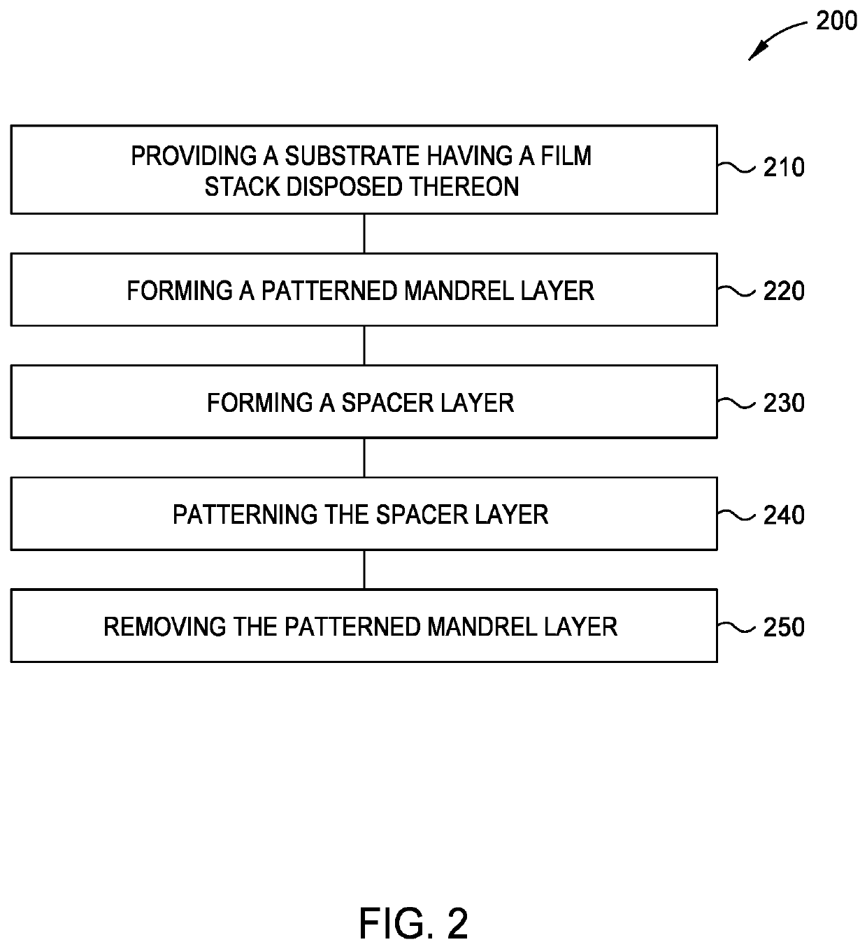
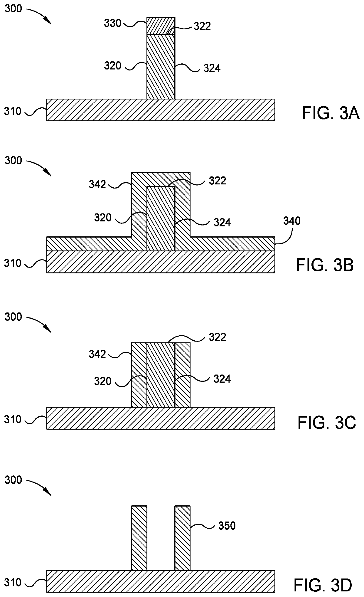
[0024]The following disclosure describes formation of high aspect ratio features. Certain details are set forth in the following description and in FIGS. 1-7D to provide a thorough understanding of various implementations of the disclosure. Other details describing well-known structures and systems often associated with formation of high aspect ratio features are not set forth in the following disclosure to avoid unnecessarily obscuring the description of the various implementations. In addition, the apparatus description described herein is illustrative and should not be construed or interpreted as limiting the scope of the implementations described herein.

[0025]Many of the details, operations, dimensions, angles and other features shown in the Figures are merely illustrative of particular implementations. Accordingly, other implementations can have other details, components, dimensions, angles and features without departing from the spirit or scope of the present disclosure. In ad...


PUM

PropertyMeasurementUnit
widthaaaaaaaaaa
widthaaaaaaaaaa
widthaaaaaaaaaa

Abstract

A method and apparatus for patterning semiconductor materials using tin-based materials as mandrels, hardmasks, and liner materials are provided. One or more implementations of the present disclosure use tin-oxide and/or tin-carbide materials as hardmask materials, mandrel materials, and/or liner material during various patterning applications. Tin-oxide or tin-carbide materials are easy to strip relative to other high selectivity materials like metal oxides (e.g., TiO2, ZrO2, HfO2, Al2O3) to avoid influencing critical dimensions and generate defects. In addition, tin-oxide and tin-carbide have low refractive index, k-value, and are transparent under 663-nm for lithography overlay.

Description

CROSS-REFERENCE TO RELATED APPLICATIONS[0001]This application claims priority to the U.S. Provisional Patent Application Ser. No. 63 / 125,576 filed Dec. 15, 2020 of which is incorporated herein by reference in its entirety.BACKGROUNDField[0002]Implementations described herein generally relate to a film stack and an etching process for etching the film stack with high selectivity and good profile control to patterning processes.Description of the Related Art[0003]Production of very large scale integration (VLSI) and ultra large scale integration (ULSI) semiconductor devices involves reliably producing submicron and smaller features. However, with the continued miniaturization of circuit technology, the dimensions of the size and pitch of circuit features, such as interconnects, have placed additional demands on processing capabilities. In order to further increase device and interconnect density, the multilevel interconnects at the heart of this technology involve precise imaging and ...

Claims


Application Information

Patent Timeline
Patent Type & Authority Applications(United States)
IPC IPC(8): H01L21/3213H01L21/02
CPCH01L21/32139H01L21/32137H01L21/02535H01L21/31144H01L21/0337H01L21/3081H01L21/31122H01L21/0332H01L21/02186H01L21/31116H01L21/022H01L21/02164H01L21/0217
Inventor LIN, YUNG-CHENLANG, CHI-IHWANG, HO-YUNG
Owner APPLIED MATERIALS INC
Why Eureka
Try Eureka