Imaging systems with integrated light shield structures

Active Publication Date: 2016-11-15
SEMICON COMPONENTS IND LLC
View PDF17 Cites 12 Cited by
  • Summary
  • Abstract
  • Description
  • Claims
  • Application Information

AI Technical Summary

Benefits of technology

The patent text is about improving imaging systems by reducing optical crosstalk and increasing quantum efficiency. This would make it better to capture images with high quality.

Problems solved by technology

In conventional imaging systems, stray light and optical crosstalk can cause unwanted image artifacts such as veiling glare, local flare, and reduced quantum efficiency.
In other situations, stray light may enter the imaging system at a high angle of incidence and may be directed on an unintended path, leading to optical crosstalk.
This type of stray light and optical crosstalk can cause bright streaks, reduced contrast, and, in some cases, undesirable color tints in dark regions of an image.

Method used


Image

  • Imaging systems with integrated light shield structures
  • Imaging systems with integrated light shield structures
  • Imaging systems with integrated light shield structures

Examples


Embodiment Construction

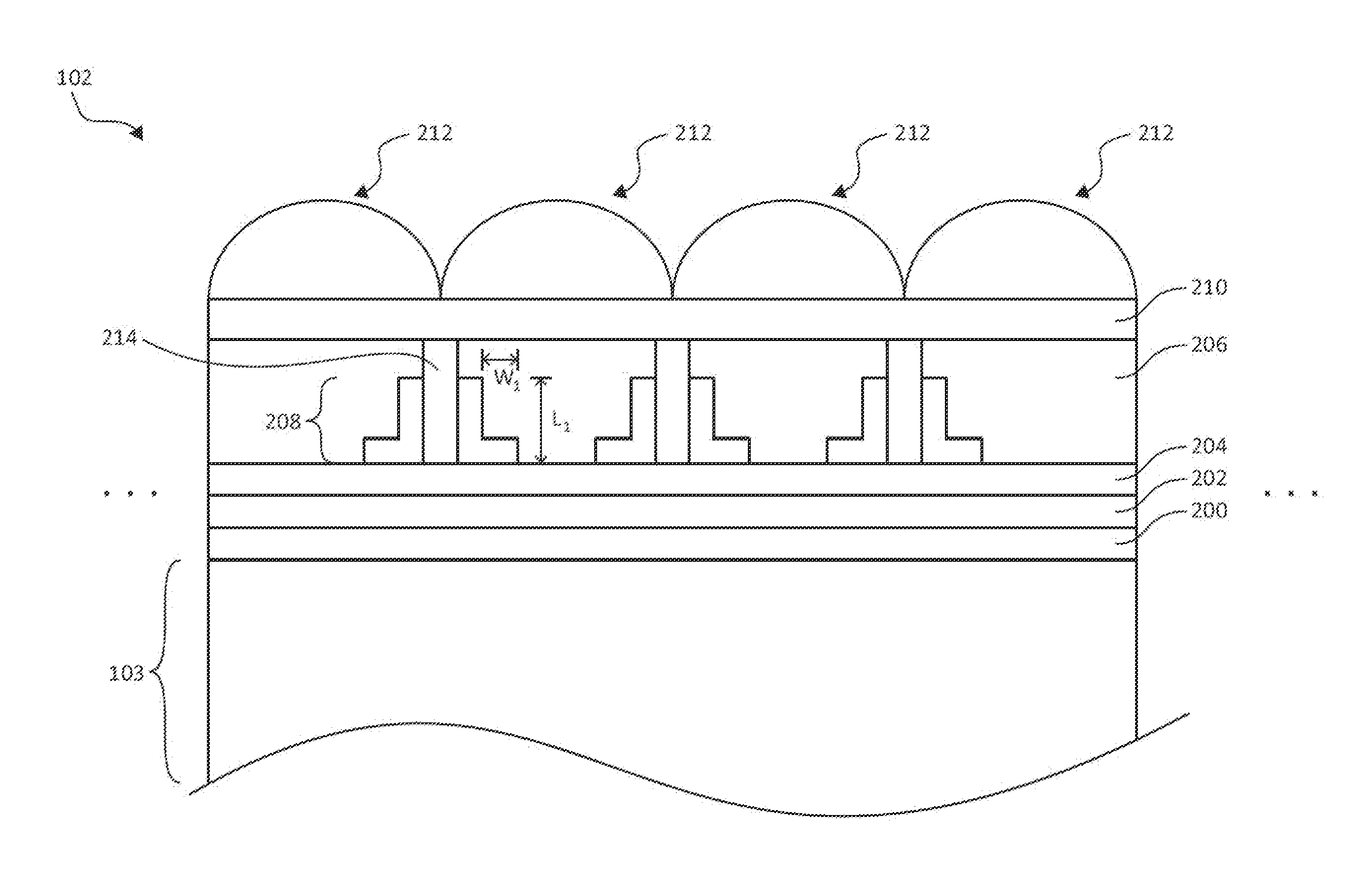
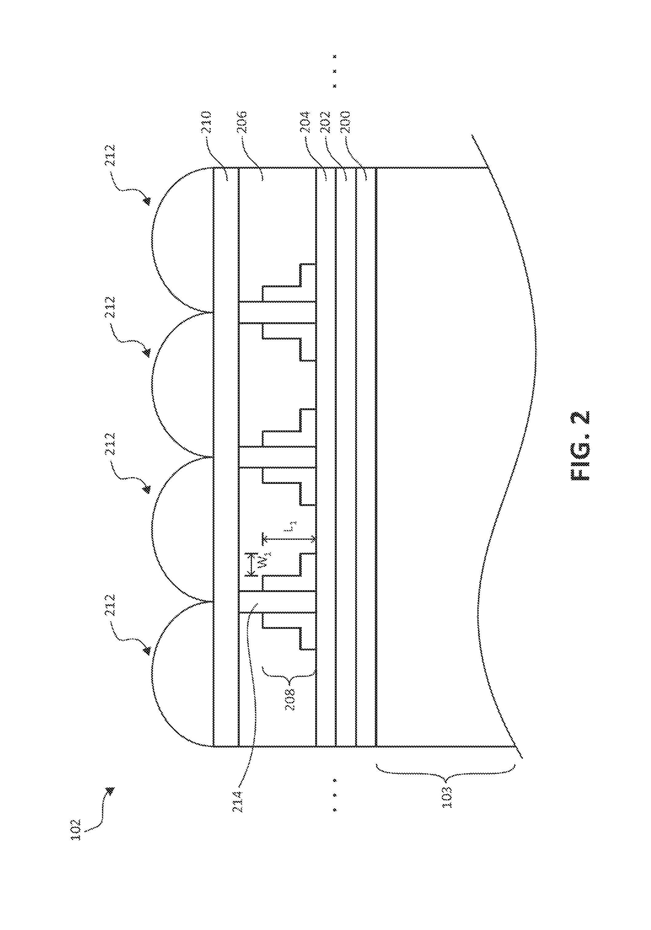
[0018]Electronic devices such as digital cameras, computers, cellular telephones, and other electronic devices include image sensors that gather incoming image light to capture an image. The image sensors may include arrays of imaging pixels. The pixels in the image sensors may include photosensitive elements such as photodiodes that convert the incoming image light into image signals. Image sensors may have any number of pixels (e.g., hundreds or thousands or more). A typical image sensor may, for example, have hundreds of thousands or millions of pixels (e.g., megapixels). Image sensors may include control circuitry such as circuitry for operating the imaging pixels and readout circuitry for reading out image signals corresponding to the electric charge generated by the photosensitive elements.

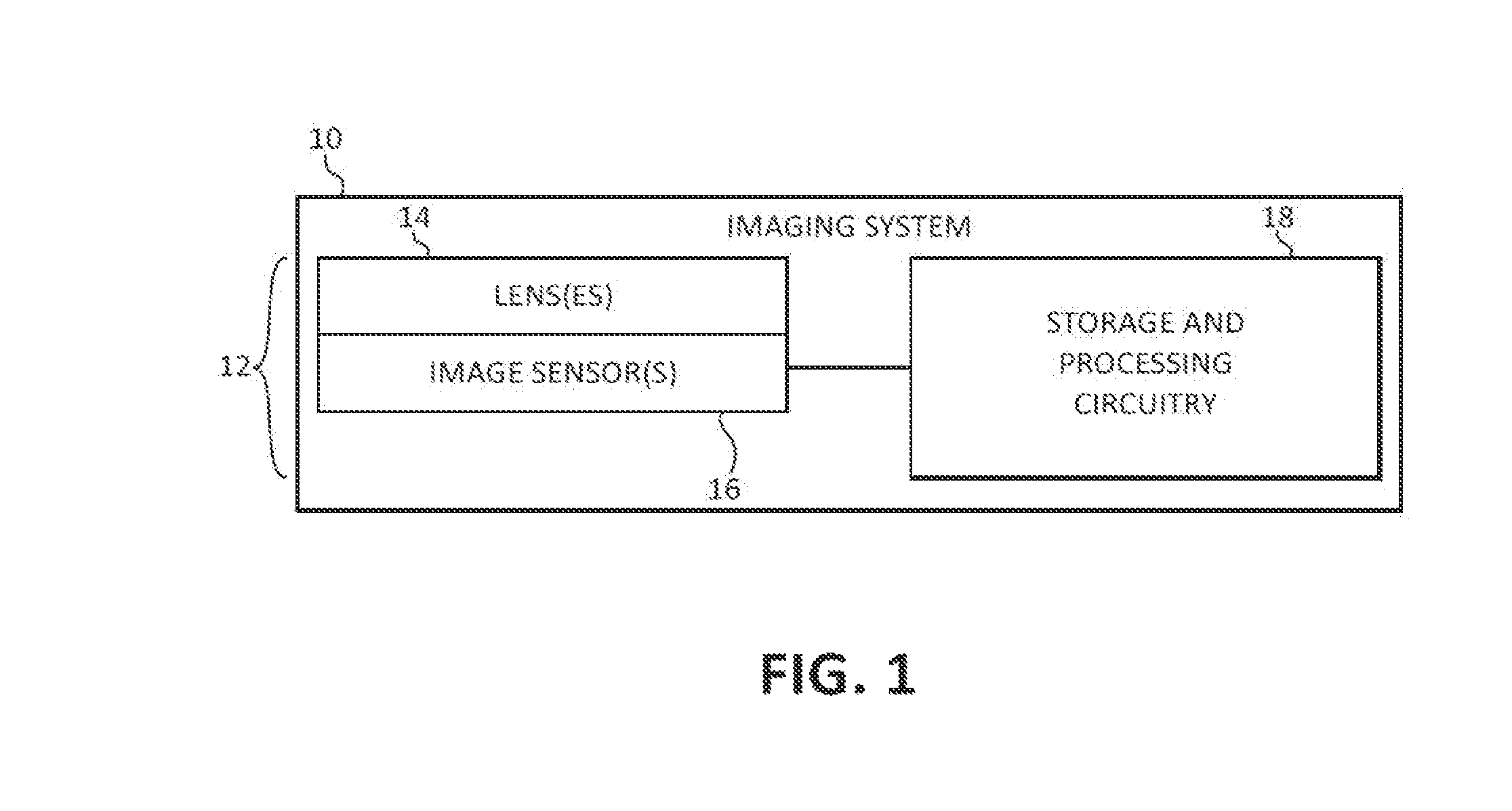
[0019]FIG. 1 is a diagram of an illustrative electronic device that uses an image sensor to capture images. Electronic device 10 of FIG. 1 may be a portable electronic device such as a camer...


PUM


Abstract

An imaging system may include an image sensor having an array of pixels. The image sensor may include an array of microlenses formed over a substrate and an array of color filter elements interposed between the microlenses and the substrate. Dielectric wall structures may be interposed between the color filter elements. Light shield structures may be formed within or on the dielectric wall structures and may be used to reduce optical crosstalk between adjacent pixels. The light shield structures may be formed on opposing sides or corners of the color filter elements and may partially or fully extend along the height of the color filter elements. In some arrangements, the light shield structures may each have a vertical portion that contacts a side surface of an adjacent color filter element and a horizontal portion that contacts a lower surface of an adjacent color filter element.

Description

BACKGROUND[0001]This relates generally to imaging systems, and more particularly to imaging systems with light shields to reduce optical crosstalk.[0002]Image sensors are commonly used in electronic devices such as cellular telephones, cameras, and computers to capture images. In a typical arrangement, an electronic device is provided with an array of image pixels and one or more lenses that focus image light onto the array of image pixels. Circuitry is commonly coupled to each pixel column for reading out image signals from the image pixels.[0003]In conventional imaging systems, stray light and optical crosstalk can cause unwanted image artifacts such as veiling glare, local flare, and reduced quantum efficiency. For example, light may enter an imaging system and may be reflected back and forth between surfaces of lens elements in the imaging system before finally reaching the array of image pixels. In other situations, stray light may enter the imaging system at a high angle of in...

Claims


Application Information

Patent Timeline
IPC IPC(8): H04N5/225H01L27/146H04N9/04
CPCH04N5/2254H04N9/045H01L27/14627H01L27/14621H01L27/14623H01L27/14603H01L27/14685H04N25/13
Inventor BOETTIGER, ULRICHPERKINS, ANDREWSULFRIDGE, MARCBORTHAKUR, SWARNAL
Owner SEMICON COMPONENTS IND LLC
Why Eureka
Try Eureka