Semiconductor optical sensor

a technology of optical sensors and semiconductors, applied in the direction of semiconductor devices, electrical equipment, radio frequency controlled devices, etc., can solve the problems of degrading the performance of the optical sensor system, and achieve the effect of reducing optical cross talk and dark curren

Active Publication Date: 2018-04-17
ARTILUX INC
View PDF4 Cites 0 Cited by
  • Summary
  • Abstract
  • Description
  • Claims
  • Application Information

AI Technical Summary

Benefits of technology

[0006]It is an object of the present disclosure to provide a semiconductor optical sensor with better light focusing and reduced optical crosstalk.
[0009]The semiconductor optical sensor according to the present disclosure can prevent the unabsorbed incident optical signal from leaking to adjacent sensing units, thus reducing optical cross talk and dark current.

Problems solved by technology

However, the performance of the optical sensor system may be degraded by the unabsorbed part of the incident optical signal after the incident optical signal passes through the photo sensitive element.

Method used


Image

  • Semiconductor optical sensor
  • Semiconductor optical sensor
  • Semiconductor optical sensor

Examples


Embodiment Construction

[0021]The present disclosure will be described in greater detail by referring to the following discussion and drawings that accompany the present disclosure. It is noted that the drawings of the present disclosure are provided for illustrative purposes and, as such, they are not drawn to scale. In the following description, numerous specific details are set forth, such as particular structures, components, materials, dimensions, processing steps and techniques, in order to provide a thorough understanding of the present disclosure. However, it will be appreciated by one of ordinary skill in the art that the present disclosure may be practiced with viable alternative process options without these specific details. In other instances, well-known structures or processing steps have not been described in detail in order to avoid obscuring the various embodiments of the present disclosure.

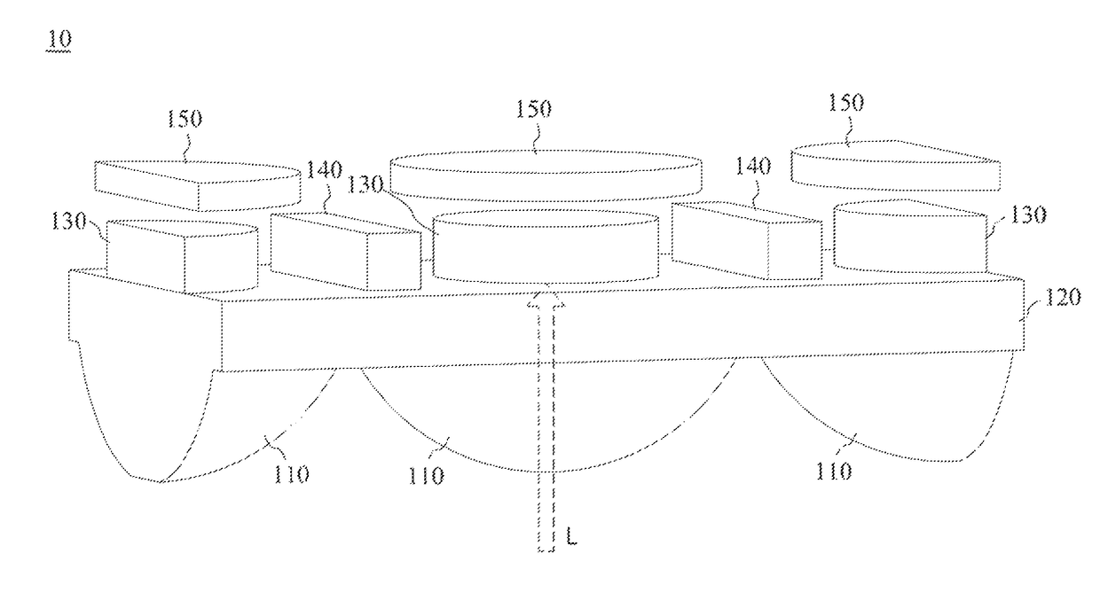
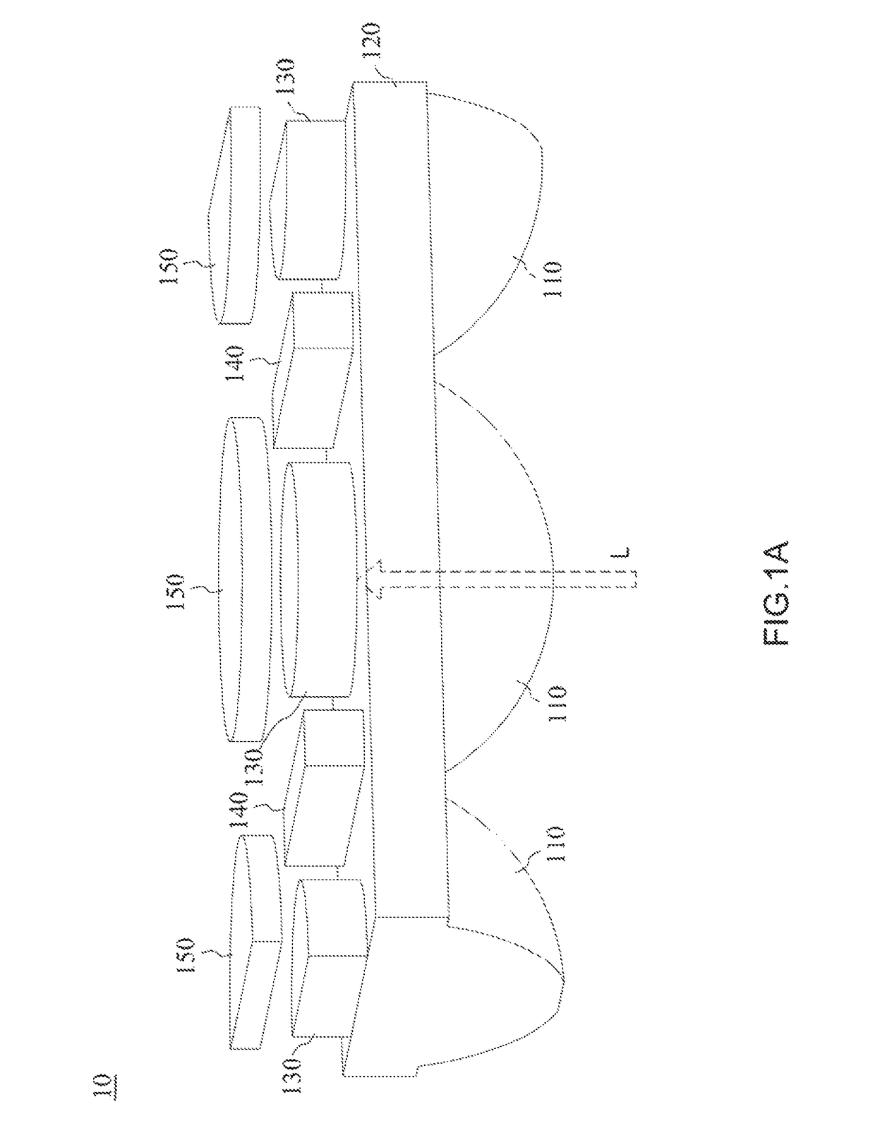
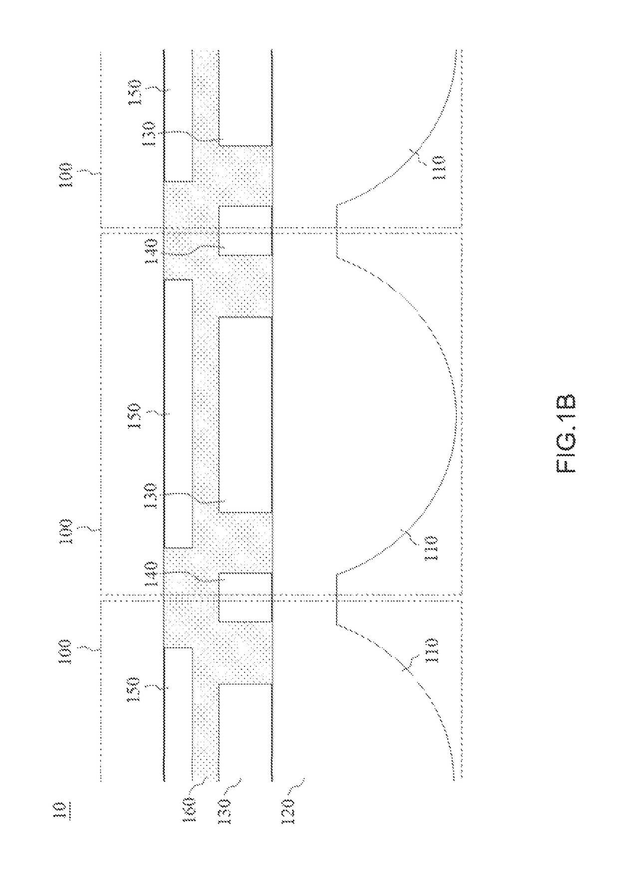
[0022]FIG. 1A shows a perspective view of the semiconductor optical sensor according to the present ...


PUM


Abstract

A semiconductor optical sensor includes a plurality of sensing units and to senses an incident optical signal to generate an electrical signal. One of the sensing units includes a substrate, an optical sensing element, a lens and an optical shielding element. The optical sensing element, whose material is different from that of the substrate, converts the incident optical signal into the electrical signal. The lens, whose material includes the same as that of the substrate, guides the incident optical signal to the optical sensing element by changing the propagation path of the incident optical signal. The optical shielding element, which surrounds the optical sensing element, alters the propagation path or propagation distance of the incident optical signal after the incident optical signal passes through the lens such that the incident optical signal will not reach an optical sensing element of an adjacent sensing unit.

Description

CROSS-REFERENCE TO RELATED APPLICATION[0001]This patent application claims the benefit of U.S. Provisional Patent Application No. 62 / 074,102, filed Nov. 3, 2014, which is incorporated by reference herein.BACKGROUND OF THE INVENTION[0002]Field of the Invention[0003]The present disclosure relates to a semiconductor optical sensor, especially to a semiconductor optical sensor with optical shielding element.[0004]Description of Prior Art[0005]The optical sensor system generally includes lens, photo sensitive element, metal routing. The incident optical signal is first focused by the lens and then converted into electric signal by the photo sensitive element. The converted electric signal is sent, through the metal routing, to other elements for further analyzing and processing. However, the performance of the optical sensor system may be degraded by the unabsorbed part of the incident optical signal after the incident optical signal passes through the photo sensitive element. In the opt...

Claims


Application Information

Patent Timeline
Patent Type & Authority Patents(United States)
IPC IPC(8): H01L31/0232H01L31/0203H01L27/146
CPCH01L31/02327H01L27/14625H01L31/0203H01L27/14629H01L27/14627
Inventor LIU, HAN-DIN
Owner ARTILUX INC
Why Eureka
Try Eureka