

Composition for metal electroplating comprising an additive for bottom-up filling of though silicon vias and interconnect features
a silicon via and additive technology, applied in the direction of liquid/solution decomposition chemical coating, coating, semiconductor devices, etc., to achieve the effect of reducing or substantially eliminating overplating, less time and effort, and high reflectivity
- Summary
- Abstract
- Description
- Claims
- Application Information
AI Technical Summary
Benefits of technology
Problems solved by technology
Method used
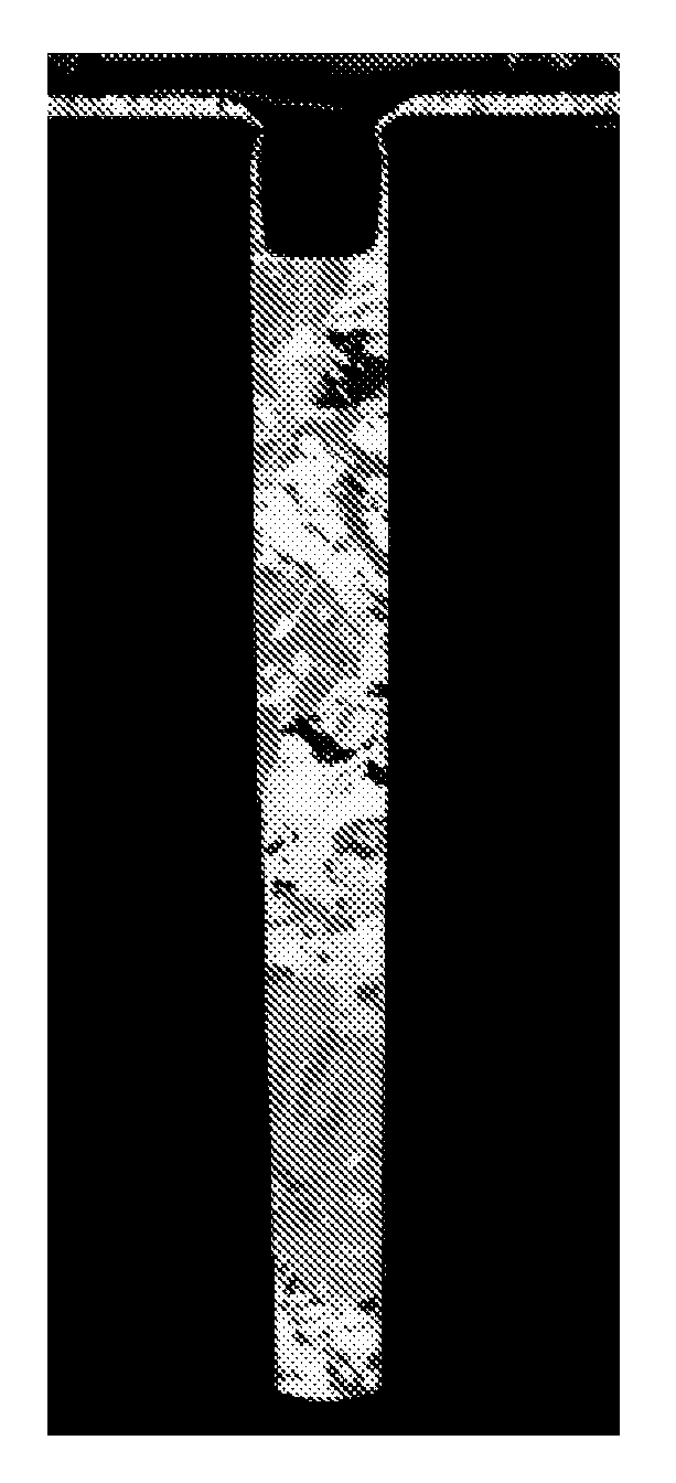
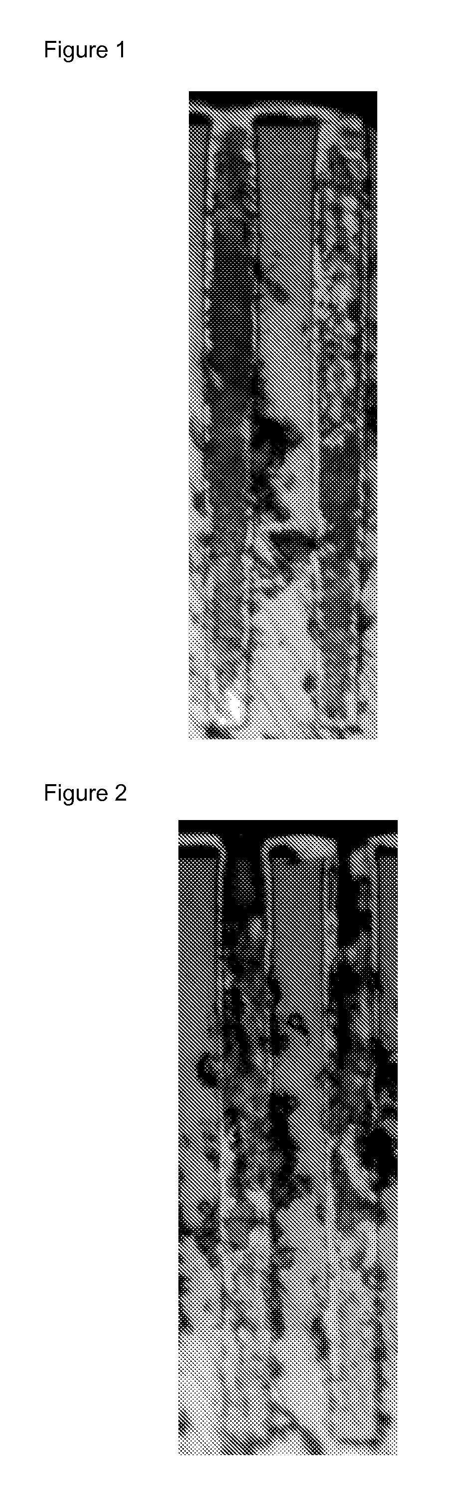
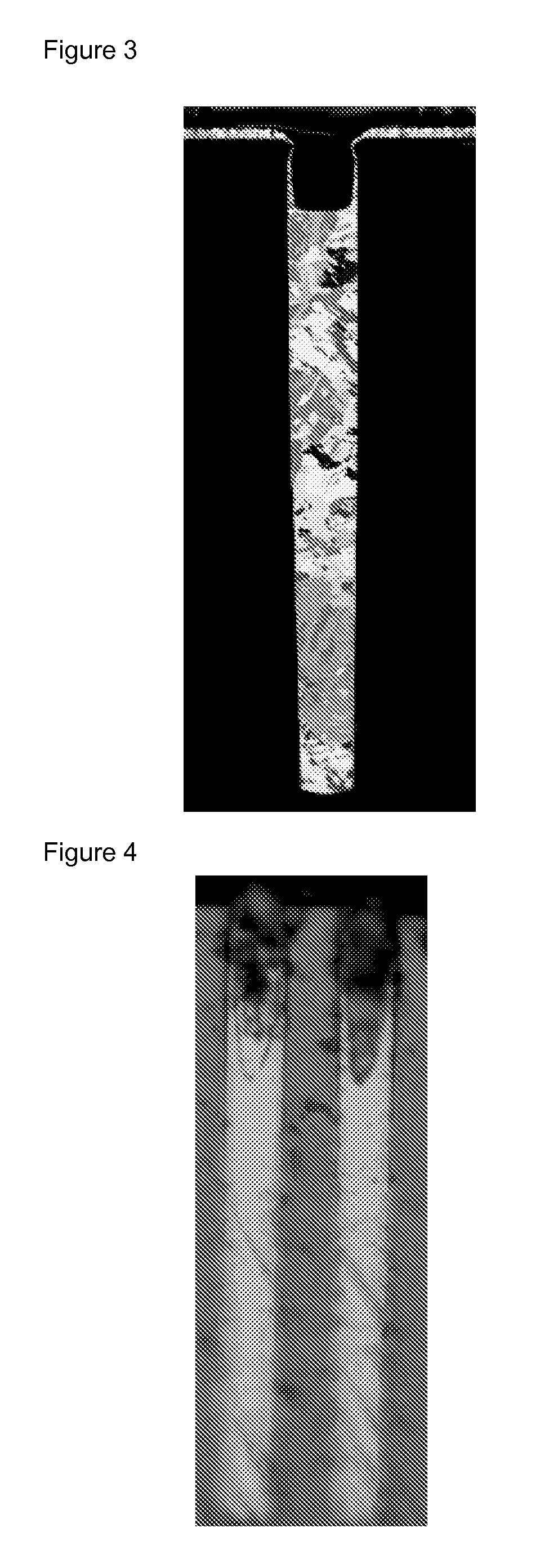
Image

Examples
example 3
Functionalized Polyaminoamide 1 from Polyaminoamide C1 and Benzyl Chloride
[0176]Polyaminoamide C1 (358 g), water (297 g) and benzyl chloride (84.9 g, 670 mmol) were placed into a 1 l apparatus and stirred at 80° C. for 6 h. One part of the resulting liquid (50 g) was washed by dichloromethane (3×20 ml) to remove unreacted benzyl chloride and the side product benzyl alcohol. Then, volatile compounds were removed at 80° C. in vacuo to give leveler 1 as a light rose solid (7.70 g) showing a nitrogen content of 12.5 g N / 100 g.
example 4
Functionalized Polyaminoamide 2 from Polyaminoamide C1 and Styrene Oxide
[0177]Polyaminoamide C1 (200 g) and water (408 g) were placed into a 1 l apparatus and heated to 100° C. during 30 min. Then, styrene oxide (11.5 g) was added dropwise during 8 min. The reaction mixture was stirred at 100° C. for 4 h, cooled to room temperature and the solvent was removed in vacuo at 80° C. Polyaminoamide 2 was obtained as a beige solid (63.5 g). Gel permeation chromatography revealed an average molecular weight of Mw=27600 g / mol and a polydispersity of Mw / Mn=1.8.
example 5
Functionalized Polyaminoamide 3 from Adipic Acid and Diethylene Triamine (Molecular Ratio 18:19), PO and Benzyl Chloride
[0178]Diethylenetriamine (820 g, 7.95 mol) was introduced into a 4 l apparatus and water (205 g) was added resulting in a temperature increase up to 54° C. The solution was heated to 60° C. and adipic acid (1100 g, 7.53 mol) was added in portions during 8 min. During this time the temperature increased up to 127° C. Then, a constant nitrogen stream was turned on, the temperature was increased to 180° C. within 30 min, and water and traces of diethylenetriamine were destilled off for 3 h at 180° C. The resulting distillate (488 g) showed an amine number of 0.48 mmol / g, indicating a content of 8.0 g diethylenetriamine in the distillate. The heating was turned off and when the temperature reached 161° C., water (1918 g) was added slowly. The reaction product was filled into a 101 Erlenmeyer flask, followed by the addition of another water portion (4800 g). The resulti...
PUM
 Abstract
Description
Claims
Application Information