

Leveler compounds
a technology of leveler compounds and compositions, applied in the field of electrolytic plating compositions, can solve the problems of high-quality metal plating, uneven metal deposits, and difficult to achieve uniform topography of substrates, and achieve reduced or substantially eliminated overplating, no suppressed local plating, and less time and effort
- Summary
- Abstract
- Description
- Claims
- Application Information
AI Technical Summary
Benefits of technology
Problems solved by technology
Method used
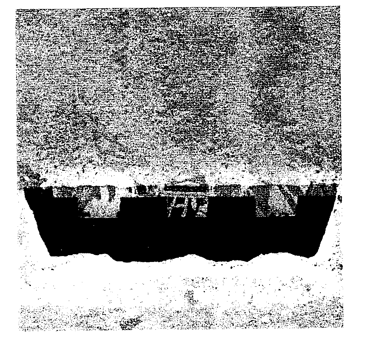
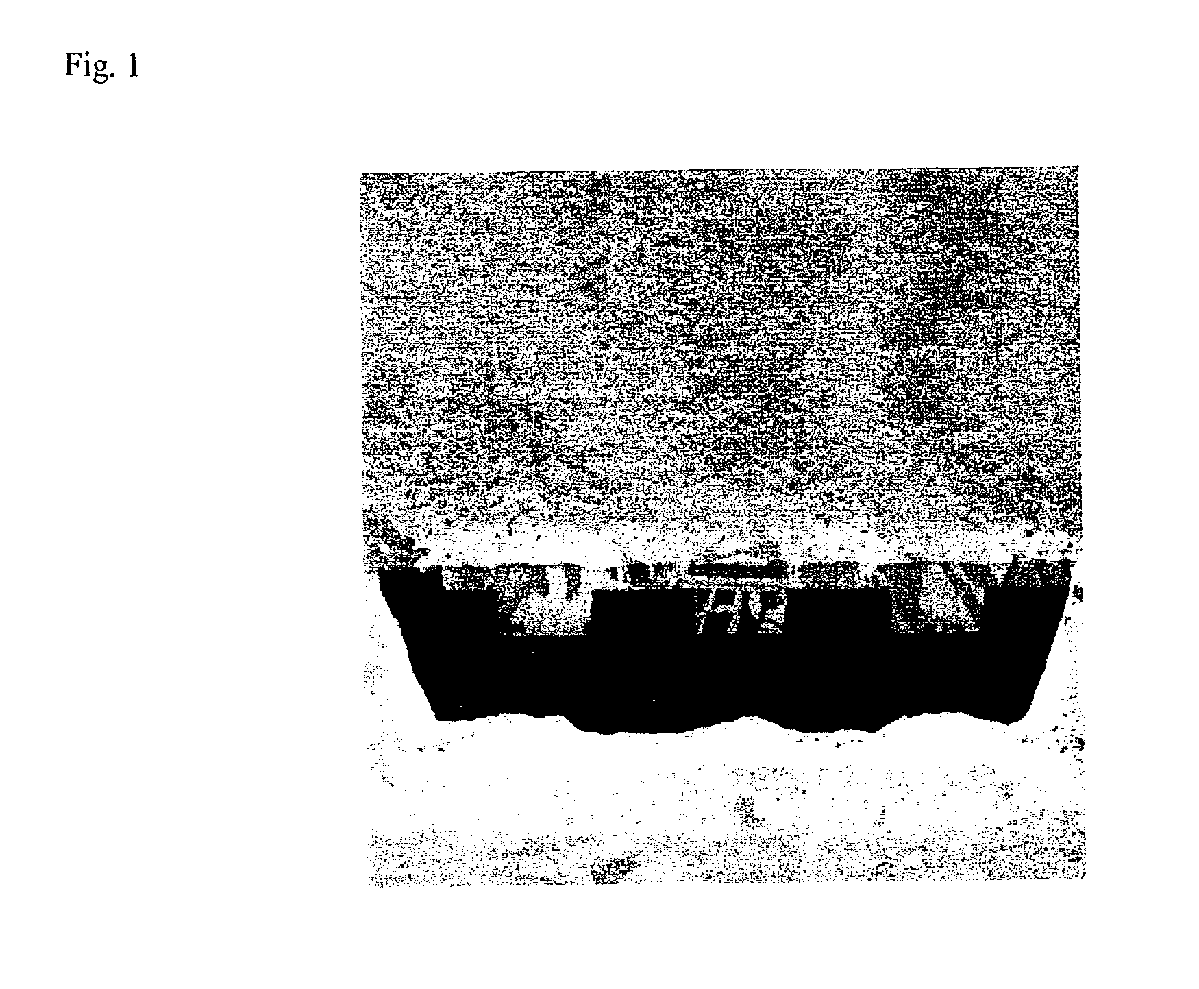
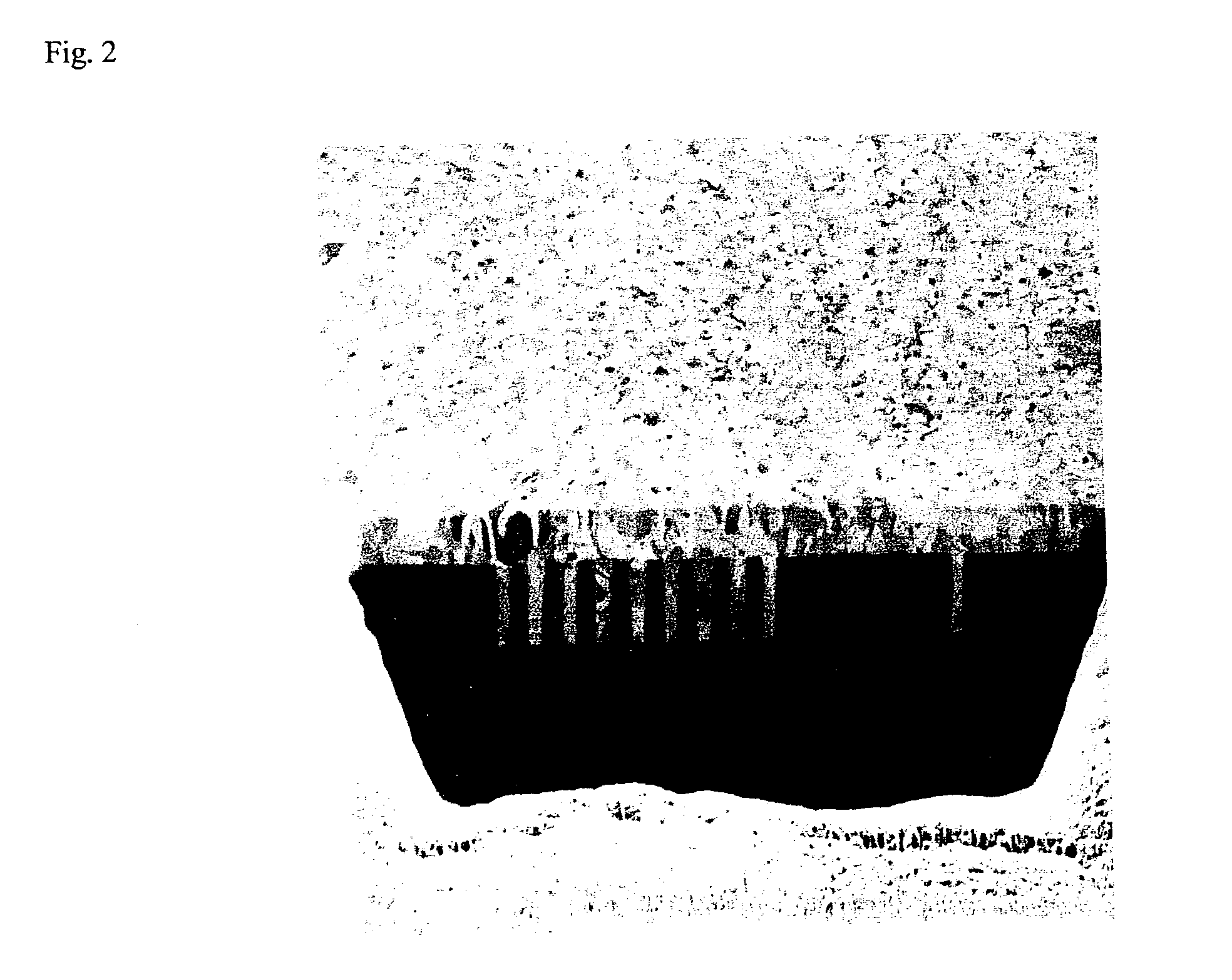
Image

Examples
example 1
[0060]A reaction product having a 2:2:1 molar ratio of imidazole:epichlorohydrin:diethylene glycol is prepared. Imidazole (2.0 g) and diethylene glycol (1.6 g) are added to a 100 mL round-bottom flask. DI water (2.5 mL) is then added to dissolve the imidazole and diethylene glycol. The flask is then placed in a water bath and is heated to 85° to 90° C. with stirring. Epichlorohydrin (2.72 g, 2.3 mol) is next added to the flask. The reaction mixture is then heated at a temperature of 90° to 98° C., with stirring, for eight hours. The heat is then turned off and the flask is allowed to cool at room temperature and is then allowed to stand overnight. A slightly yellow waxy solid is obtained, which can be used without further purification. This solid is analyzed by high pressure liquid chromatography (“HPLC”) to show a polymeric reaction is obtained.
examples 2 – 10
EXAMPLES 2–10
[0061]The procedure of Example 1 is repeated except that the specific alkylene oxide used and the ratio of the reactants are varied. The specific alkylene oxide compound used and the ratios of reactants are reported in Table 1.
[0062]
TABLE 1Molar Ratio ofImidazole:MolecularEpichlorohydrin:ExamplesAlkylene OxideWeightAlkylene Oxide2Diethylene glycol1:1:1 3Diethylene glycol0.5:1:1 4Polyethylene glycol10001:1:0.5 5Polyethylene glycol30001:1:0.256EO / PO / EO copolymer11001:1:0.257EO / PO / EO copolymer25001:1:0.258EO / PO / EO copolymer18501:1:0.5 9EO / PO / EO copolymer22001:1:0.5 10 EO / PO / EO copolymer29001:1:0.25
example 11
[0063]The procedure of Example 1 is repeated except that pyridine is used instead of imidazole.
PUM
| Property | Measurement | Unit |
|---|---|---|
| concentration | aaaaa | aaaaa |
| concentration | aaaaa | aaaaa |
| size | aaaaa | aaaaa |
Abstract
Description
Claims
Application Information