ESD protection control circuit and system

a protection control circuit and control circuit technology, applied in emergency protective arrangements, electrical equipment, and circuit elements, etc., can solve the problems of increasing the esd tolerance capability of circuit elements, increasing the quantity of environmental static electricity, and increasing the element dimension. , to achieve the effect of improving esd protection

Active Publication Date: 2017-06-27
NOVATEK MICROELECTRONICS CORP
View PDF8 Cites 0 Cited by
  • Summary
  • Abstract
  • Description
  • Claims
  • Application Information

AI Technical Summary

Benefits of technology

[0010]The present invention further discloses an ESD protection system for an output pad of an IC. The ESD protection system comprises an output driver, a previous stage, an ESD protection cell and a control switch. The output driver, coupled to the output pad, comprises an output transistor for outputting power or signals to the output pad. The previous stage, coupled to the output driver, is used for receiving power from a power supply terminal. The ESD protection cell is coupled to the output pad. The control switch, for improving ESD protection on the output pad when closed, comprises a first connection terminal, coupled to a gate terminal of the first output transistor; a second connection terminal, coupled to a ground terminal; and a control terminal, coupled to the power supply terminal.

Problems solved by technology

Reliability issues also become significant with decreasing element dimensions.
Since the circuit elements in advanced processes have smaller dimensions, the ESD tolerance capability of the circuit elements becomes worse, while the quantity of environmental static electricity still remains.
Therefore, the circuit elements may be damaged by ESD more easily.
However, the layout rule with higher ESD tolerance capability always requires a larger area and is thereby accompanied by poor performance.
However, there is a parasitic capacitance Cgd between the gate terminal and drain terminal of the output transistor 100.
As can be seen, the conventional ESD protection techniques are not satisfactory.

Method used


Image

  • ESD protection control circuit and system
  • ESD protection control circuit and system
  • ESD protection control circuit and system

Examples


Embodiment Construction

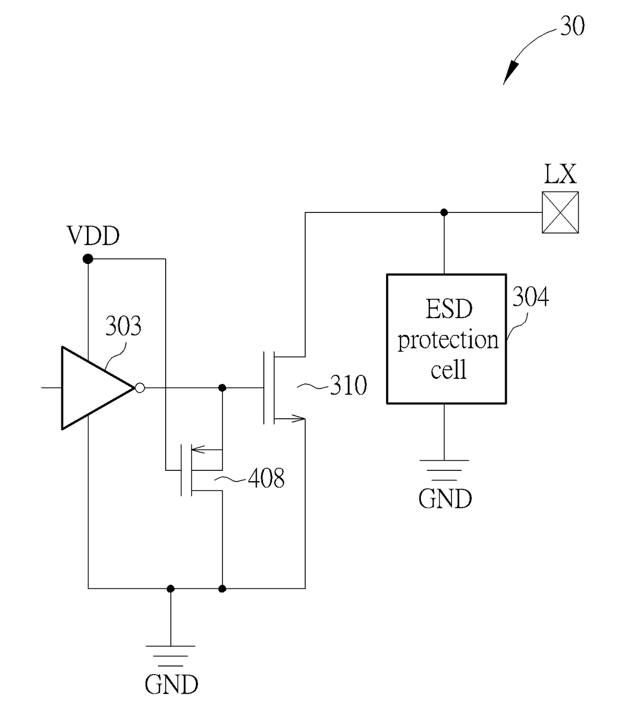
[0018]Please refer to FIG. 3A and FIG. 3B, which are schematic diagrams of an electrostatic discharge (ESD) protection system 30 according to an embodiment of the present invention. The ESD protection system 30 includes an output pad LX of an integrated circuit (IC), an output driver 300, a previous stage 302, an ESD protection cell 304 and a control switch 308. The output driver 300, coupled to the output pad LX, includes an output transistor 310 for outputting power or signals to the output pad LX. For example, if the output transistor 310 is a power transistor, the output transistor 310 will output power to the output pad LX. The previous stage 302, coupled to the output driver 300, receives power from a power supply terminal VDD and drives the output transistor 310 to output the power or signals. The previous stage 302 includes an inverter 303 to output control signals to drive the output transistor 310. The ESD protection cell 304, coupled to the output pad LX, is externally co...


PUM


Abstract

An electrostatic discharge (ESD) protection control circuit for an output pad of an integrated circuit includes an output driver and a control switch. The output driver, coupled to the output pad, includes a first output transistor for outputting power or signals to the output pad. The control switch, for improving ESD protection on the output pad when closed, includes a first connection terminal, coupled to a gate terminal of the first output transistor; a second connection terminal, coupled to a ground terminal; and a control terminal, coupled to a first power supply terminal.

Description

BACKGROUND OF THE INVENTION[0001]1. Field of the Invention[0002]The present invention relates to an electrostatic discharge (ESD) protection control circuit and system, and more particularly, to an ESD protection control circuit and system capable of improving ESD protection on an output pad of an integrated circuit.[0003]2. Description of the Prior Art[0004]With advancement in semiconductor process technology, the dimension of circuit elements shrinks to a submicron level, which increases performance and operation speed of integrated circuits (ICs). Reliability issues also become significant with decreasing element dimensions. Among these issues, electrostatic discharge (ESD) is one of the most important issues to be dealt with. Since the circuit elements in advanced processes have smaller dimensions, the ESD tolerance capability of the circuit elements becomes worse, while the quantity of environmental static electricity still remains. Therefore, the circuit elements may be damage...

Claims


Application Information

Patent Timeline
Patent Type & Authority Patents(United States)
IPC IPC(8): H02H9/04
CPCH02H9/04H02H9/046H01L27/0251
Inventor CHEN, LU-ANSUNG, TUNG-HAOWU, KUN-JHENG
Owner NOVATEK MICROELECTRONICS CORP
Why Eureka
Try Eureka