Layout structure for electrostatic discharge protection

a technology of electrostatic discharge and layout structure, which is applied in the direction of diodes, semiconductor devices, electrical apparatus, etc., can solve the problems of ggnmos not providing sufficient esd protection, affecting the stability and reliability of integrated circuits, and electrostatic discharge, etc., to achieve the effect of increasing the circuit size and improving the esd protection

Active Publication Date: 2017-03-23
UNITED MICROELECTRONICS CORP
View PDF8 Cites 0 Cited by
  • Summary
  • Abstract
  • Description
  • Claims
  • Application Information

AI Technical Summary

Benefits of technology

[0006]The disclosure is directed to a layout structure. According to the embodiments of the present disclosure, the third doped region is formed in the substrate and adjacent to the second doped region, the two regions having complimentary conductivities, such that a diode formed from the third doped region and the second doped region is advantageous to the dissipation of ESD current, thereby improving the ESD protection without largely increasing the circuit size.

Problems solved by technology

Electrostatic discharge (ESD) has become one of the major issues affecting the stability and reliability of integrated circuits (IC).
However, the GGNMOS still cannot provide sufficient ESD protection.

Method used


Image

  • Layout structure for electrostatic discharge protection
  • Layout structure for electrostatic discharge protection
  • Layout structure for electrostatic discharge protection

Examples


Embodiment Construction

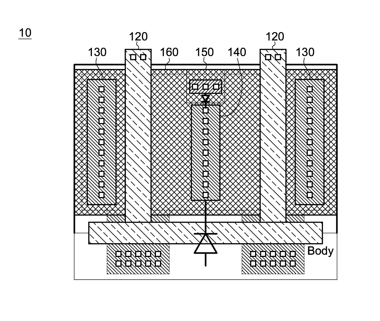
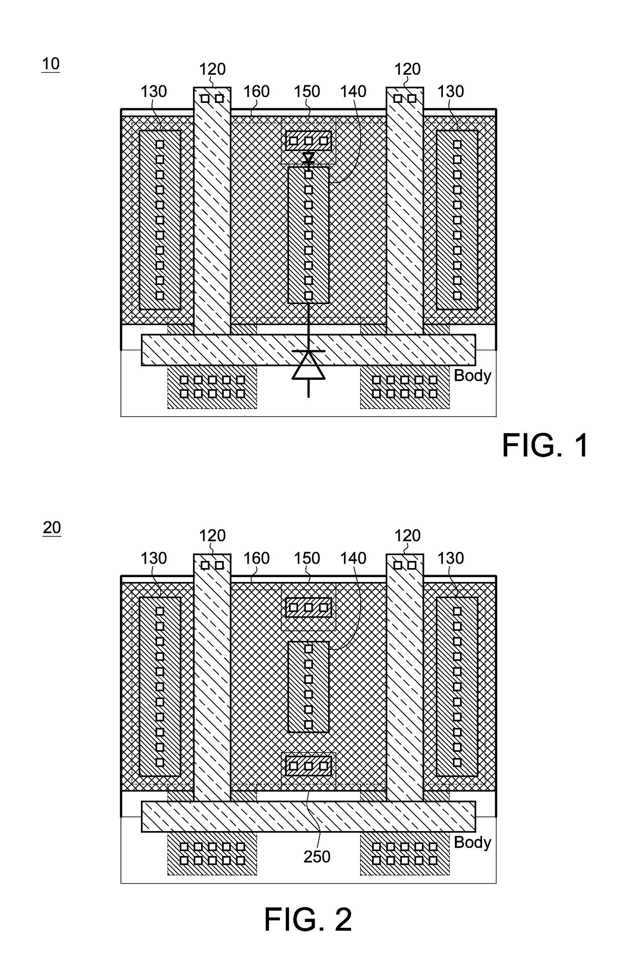
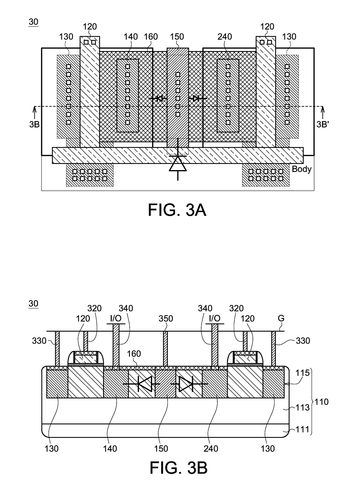
[0019]According to the embodiments of the present disclosure, in the layout structure, the third doped region is formed in the substrate and adjacent to the second doped region, the two regions having complimentary conductivities, such that a diode formed from the third doped region and the second doped region is advantageous to the dissipation of ESD current, thereby improving the ESD protection without largely increasing the circuit size. The identical or similar elements of the embodiments are designated with the same reference numerals. It is to be noted that the drawings are simplified for clearly describing the embodiments, and the details of the structures of the embodiments are for exemplification only, not for limiting the scope of protection of the disclosure. Ones having ordinary skills in the art may modify or change the structures according to the embodiments of the present disclosure.

[0020]FIG. 1 is a top view of a layout structure 10 according to an embodiment of the ...


PUM


Abstract

A layout structure is provided. The layout structure includes a substrate, a gate conductive layer, a first doped region having a first conductivity, a second doped region having the first conductivity, and a third doped region having a second conductivity. The gate conductive layer is formed on the substrate. The first doped region the second doped region are formed in the substrate and located at two sides of the gate conductive layer. The third doped region is formed in the substrate and adjacent to the second doped region. The third doped region and the second doped region form a diode. The gate conductive layer, the first doped region, and the third doped region are connected to ground, and the second doped region is connected to an input/output pad.

Description

BACKGROUND[0001]Technical Field[0002]The disclosure relates in general to a layout structure, and more particularly to a layout structure with improved electrostatic discharge protection (ESD).[0003]Description of the Related Art[0004]Electrostatic discharge (ESD) has become one of the major issues affecting the stability and reliability of integrated circuits (IC). Despite the thermal dissipation disadvantages caused by the presence of a buried oxide in silicon-on-insulator (SOI) technology, a grounded-gate N MOS (GGNMOS) using SOI technology has been applied for improving ESD protection due to the advantages of low leakage, low capacitance, latch-up free, and etc.[0005]However, the GGNMOS still cannot provide sufficient ESD protection. Therefore, there is still a continuing need to provide improved ESD protection of SOI technology.SUMMARY OF THE INVENTION[0006]The disclosure is directed to a layout structure. According to the embodiments of the present disclosure, the third doped ...

Claims


Application Information

Patent Timeline
Patent Type & Authority Applications(United States)
IPC IPC(8): H01L27/02
CPCH01L27/0207H01L27/0266H01L27/0255H01L27/1203H01L28/00
Inventor TSENG, PEI-SHANLIAO, YU-CHENGCHANG, PING-CHENTANG, TIEN-HAOSU, KUAN-CHENG
Owner UNITED MICROELECTRONICS CORP
Why Eureka
Try Eureka