ESD protection circuit

a protection circuit and circuit technology, applied in the field of circuits, can solve the problems of increasing the capacitance affecting and asymmetric behavior of the esd circuit, and achieve the effect of improving the control of the doping profile of the bipolar transistor

Active Publication Date: 2014-11-18
AMPLEON NETHERLANDS
View PDF10 Cites 0 Cited by
  • Summary
  • Abstract
  • Description
  • Claims
  • Application Information

AI Technical Summary

Benefits of technology

[0008]The present invention seeks to provide a transistor for use in power amplifiers having improved ESD protection.
[0010]The use of (NPN) bipolar transistors in such a configuration ensures a symmetrical ESD protection, i.e. the ESD protection is triggered at both positive and negative gate-source voltages (Vgs) of the transistor to be protected, e.g. a RF-LDMOS transistor in a power amplifier. In addition, by providing dual-sided ESD protection implemented with (NPN) bipolar transistors, the ESD protection circuit is capable of handling higher current densities compared to the aforementioned prior art solutions.
[0012]Advantageously, the circuit comprises first and second MOS transistors coupled in series between the input signal line and ground, wherein the gate of the first MOS transistor is connected to the input signal line and the gate of the second MOS transistor is connected to ground, and wherein a node between the first bipolar transistor and the second bipolar transistor is connected to a node between the first MOS transistor and the second MOS transistor. Such transistors, which preferably are NMOS transistors and more preferably are n-type LDMOS transistors, act as diodes in parallel to the N-well and P-well diodes of the bipolar transistors. The inclusion of such MOS transistors in the ESD circuit in the vicinity of the bipolar transistors improves the control over the doping profiles of the bipolar transistors.

Problems solved by technology

A drawback of this approach is that its behavior is asymmetrical, i.e. (intentional) negative voltages occurring on the control terminal of the ggnMOS force this device into a conductive state.
This can cause problems in a bias circuit connected to the LDMOS transistor.
However, these solutions are unsatisfactory where silicon real estate is at a premium as for such ESD protection circuits typically have a modest current density such that they must cover a relatively large area to be able to sufficiently cope with ESD events.
A further drawback of such relatively area intensive solutions is that they increase the capacitance of the ESD circuit, which is also undesirable.

Method used


Image

  • ESD protection circuit
  • ESD protection circuit
  • ESD protection circuit

Examples


Embodiment Construction

[0013]Embodiments of the invention are described in more detail and by way of non-limiting examples with reference to the accompanying drawings, wherein:

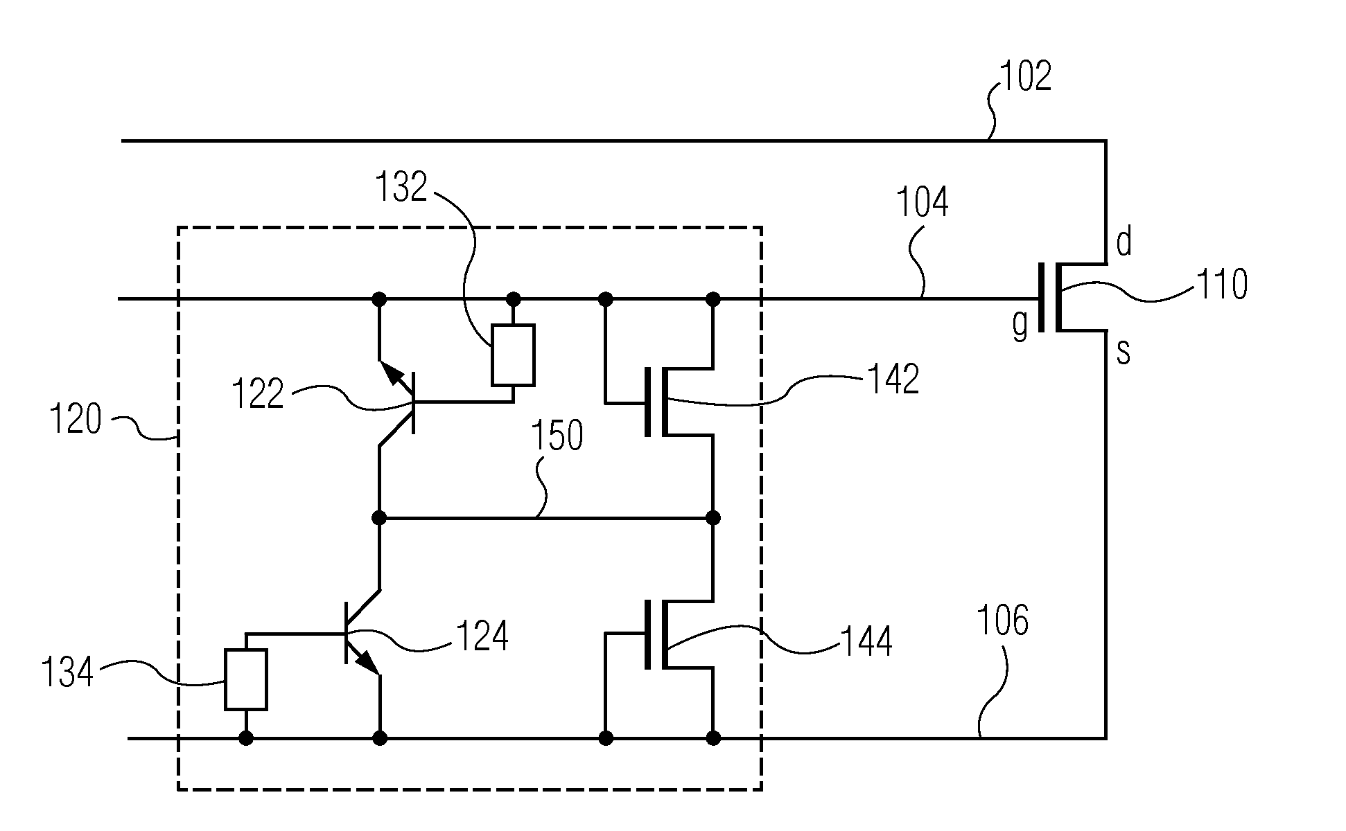
[0014]FIG. 1 schematically depicts a circuit according to an embodiment of the present invention;

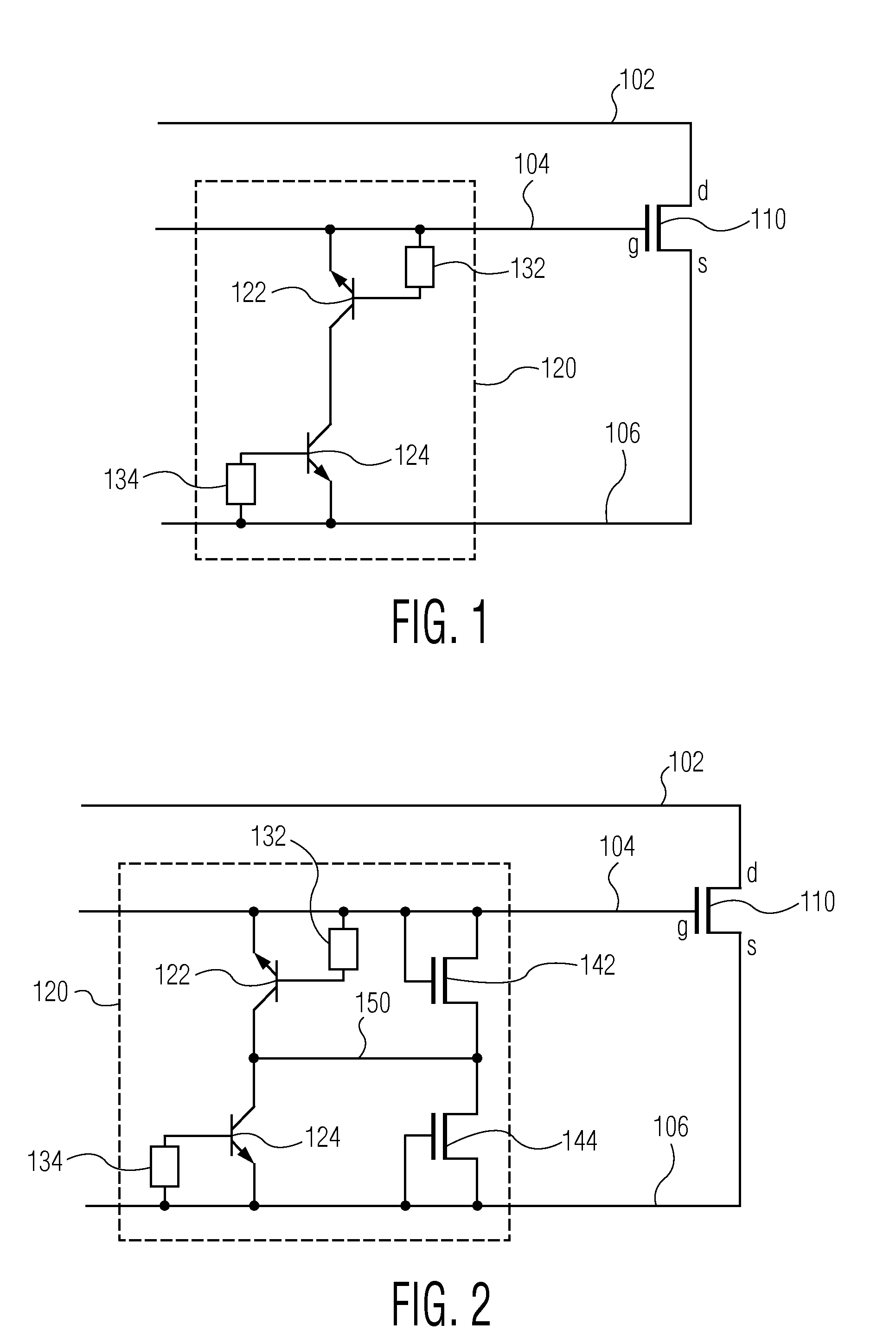
[0015]FIG. 2 schematically depicts a circuit according to another embodiment of the present invention;

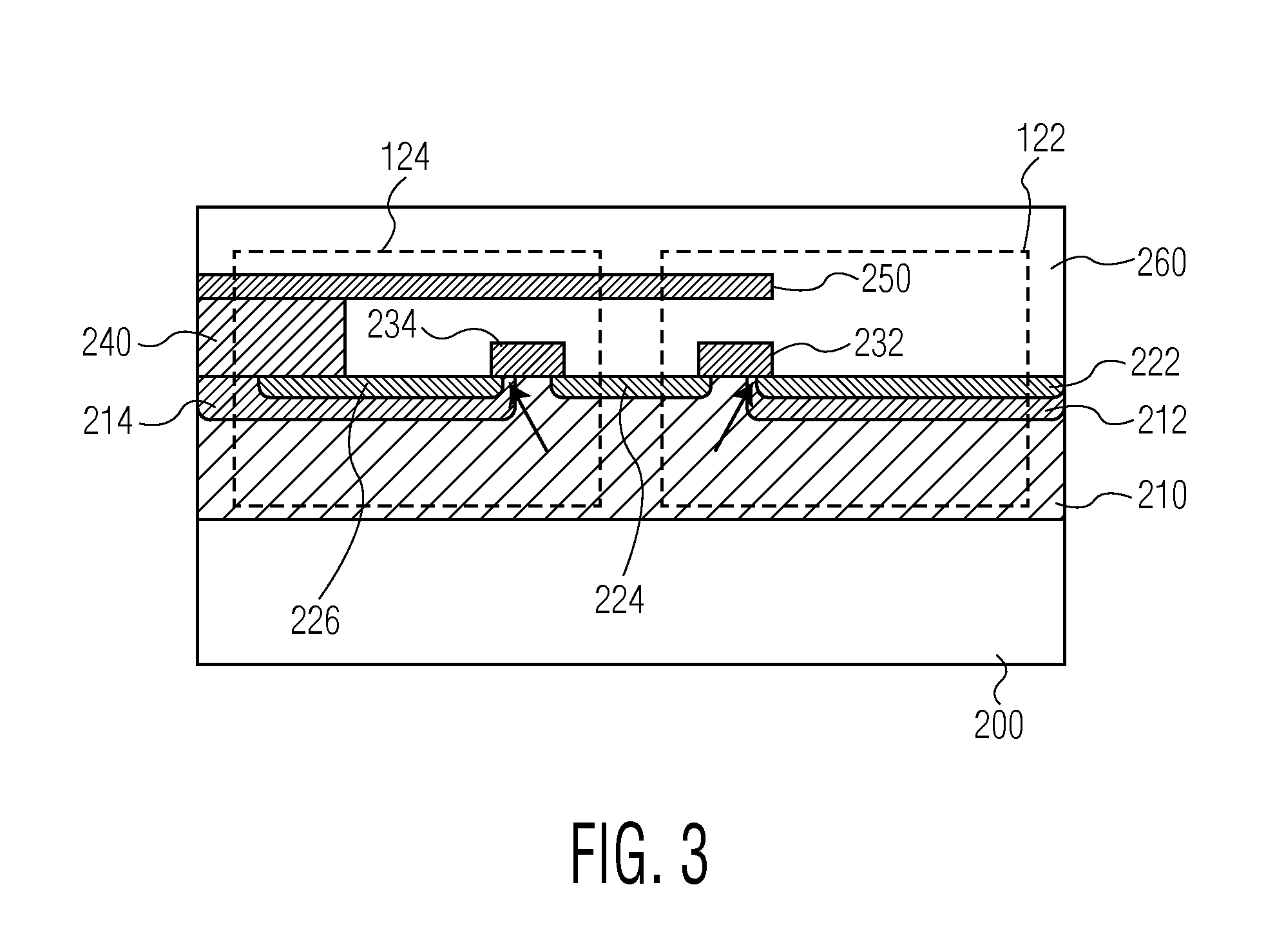
[0016]FIG. 3 schematically depicts an aspect of the layout of a circuit according to an embodiment of the present invention in more detail; and

[0017]FIG. 4 depicts the measurement results of the ESD protection behavior of a circuit in accordance with an embodiment of the present invention.

DETAILED DESCRIPTION OF THE DRAWINGS

[0018]It should be understood that the Figures are merely schematic and are not drawn to scale. It should also be understood that the same reference numerals are used throughout the Figures to indicate the same or similar parts.

[0019]FIG. 1 depicts a first embodiment of the present invention, in which an integrated ci...


PUM


Abstract

Disclosed is a circuit (100) comprising a transistor (110) coupled between a supply voltage line (102) and ground (106), the transistor comprising a control terminal coupled to a input signal line (104), the circuit further comprising first and second bipolar transistors (122, 124) coupled in series between the input signal line (104) and ground (106), wherein the base of the first bipolar transistor is connected to the input signal line and the base of the second bipolar transistor is connected to ground.

Description

CROSS-REFERENCE TO RELATED APPLICATIONS[0001]This application claims the priority under 35 U.S.C. §119 of European patent application no. 11163258.4, filed on Apr. 20, 2011, the contents of which are incorporated by reference herein.FIELD OF THE INVENTION[0002]The present invention relates to a circuit comprising a transistor coupled between a supply voltage line and ground, the transistor comprising a control terminal coupled to an input signal line.BACKGROUND OF THE INVENTION[0003]ESD (electrostatic discharge) protection is commonly applied to circuits to protect circuit elements from damage in case of an ESD event on a control terminal of the circuit element. For instance, in CMOS circuits the use of so-called grounded gate nMOS (ggNMOS) transistors coupled between the control terminal of the circuit element to be protected and ground are commonly used for such ESD protection. The ggNMOS transistor is typically implemented with a relatively large width to length (W / L) ratio, in w...

Claims


Application Information

Patent Timeline
Patent Type & Authority Patents(United States)
IPC IPC(8): H01L27/02H03K19/003H02H9/04
CPCH01L27/0259H03K19/00315H02H9/044
Inventor DE, BOET, JOHANNES, ADRIANUS, MARIA
Owner AMPLEON NETHERLANDS
Why Eureka
Try Eureka