Electronic device including electrically conductive body for ESD protection and related methods

a technology of esd protection and electrical conductivity, applied in the field of electrostatic discharge protection devices, can solve the problems of esd damage to the transistor device, and the transistor device may be the most susceptible to esd damage during handling, so as to reduce the possibility of esd damage

Active Publication Date: 2014-03-18
HARRIS GLOBAL COMM INC
View PDF4 Cites 0 Cited by
  • Summary
  • Abstract
  • Description
  • Claims
  • Application Information

AI Technical Summary

Benefits of technology

[0007]In view of the foregoing background, it is therefore an object of the present invention to reduce the possibility of ESD damage during transport and / or installation of a transistor device.
[0008]This and other objects, features, and advantages in accordance with the present invention are provided by an electronic device that includes a transistor device including a transistor package and a plurality of transistor terminals extending outwardly therefrom. The electronic device also includes an electrically conductive body removably coupled to and shorting together the plurality of transistor terminals for electrostatic discharge (ESD) protection. Accordingly, the electronic device provides increased ESD protection, for example, during transport and installation.

Problems solved by technology

An ESD as low as 250 volts may destroy the transistor device or damage the transistor device so that is fails.
A transistor device may be most susceptible to ESD damage during handling, which may include, for example, packaging by the manufacturer, removal from the manufacturer's packaging, and / or installation in a an electronic circuit.
A transistor device may be most susceptible to damage from gate-to-source and drain-to-source potentials, for example.
However, the transistor device is eventually removed from the conductive packaging prior to being installed, which may expose the transistor device to ESD damage.

Method used


Image

  • Electronic device including electrically conductive body for ESD protection and related methods
  • Electronic device including electrically conductive body for ESD protection and related methods
  • Electronic device including electrically conductive body for ESD protection and related methods

Examples


Embodiment Construction

[0017]The present invention will now be described more fully hereinafter with reference to the accompanying drawings, in which preferred embodiments of the invention are shown. This invention may, however, be embodied in many different forms and should not be construed as limited to the embodiments set forth herein. Rather, these embodiments are provided so that this disclosure will be thorough and complete, and will fully convey the scope of the invention to those skilled in the art. Like numbers refer to like elements throughout, and prime notation is used to indicate similar elements in alternative embodiments.

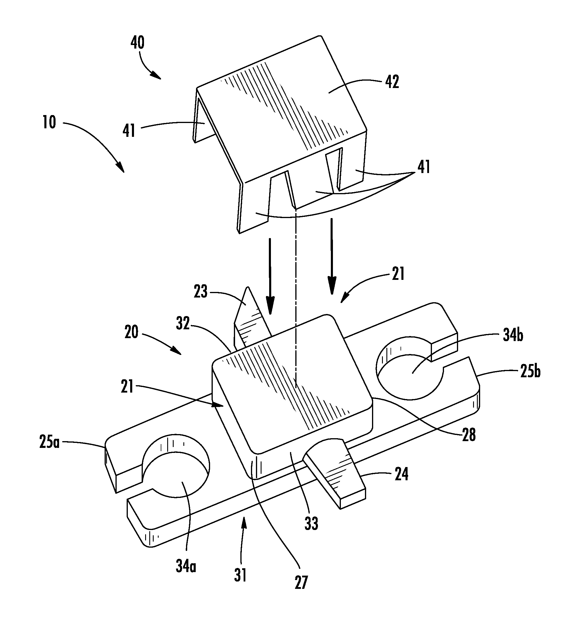
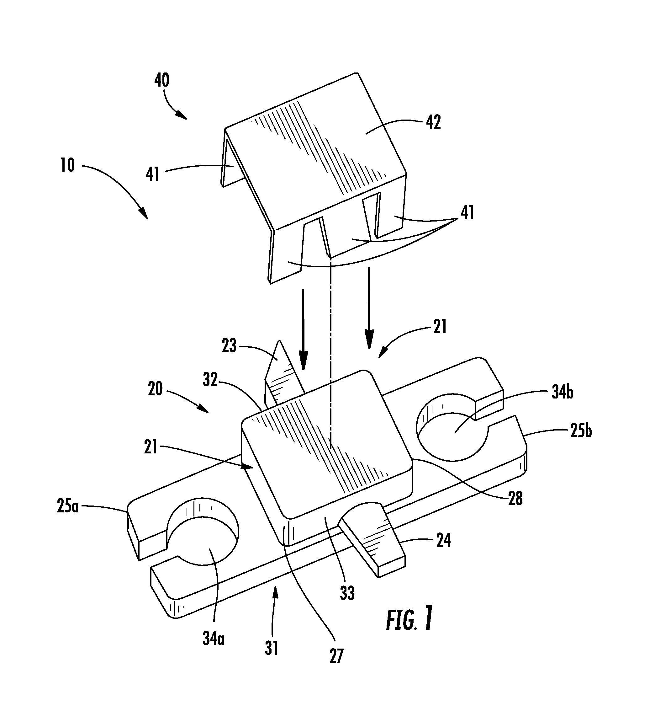
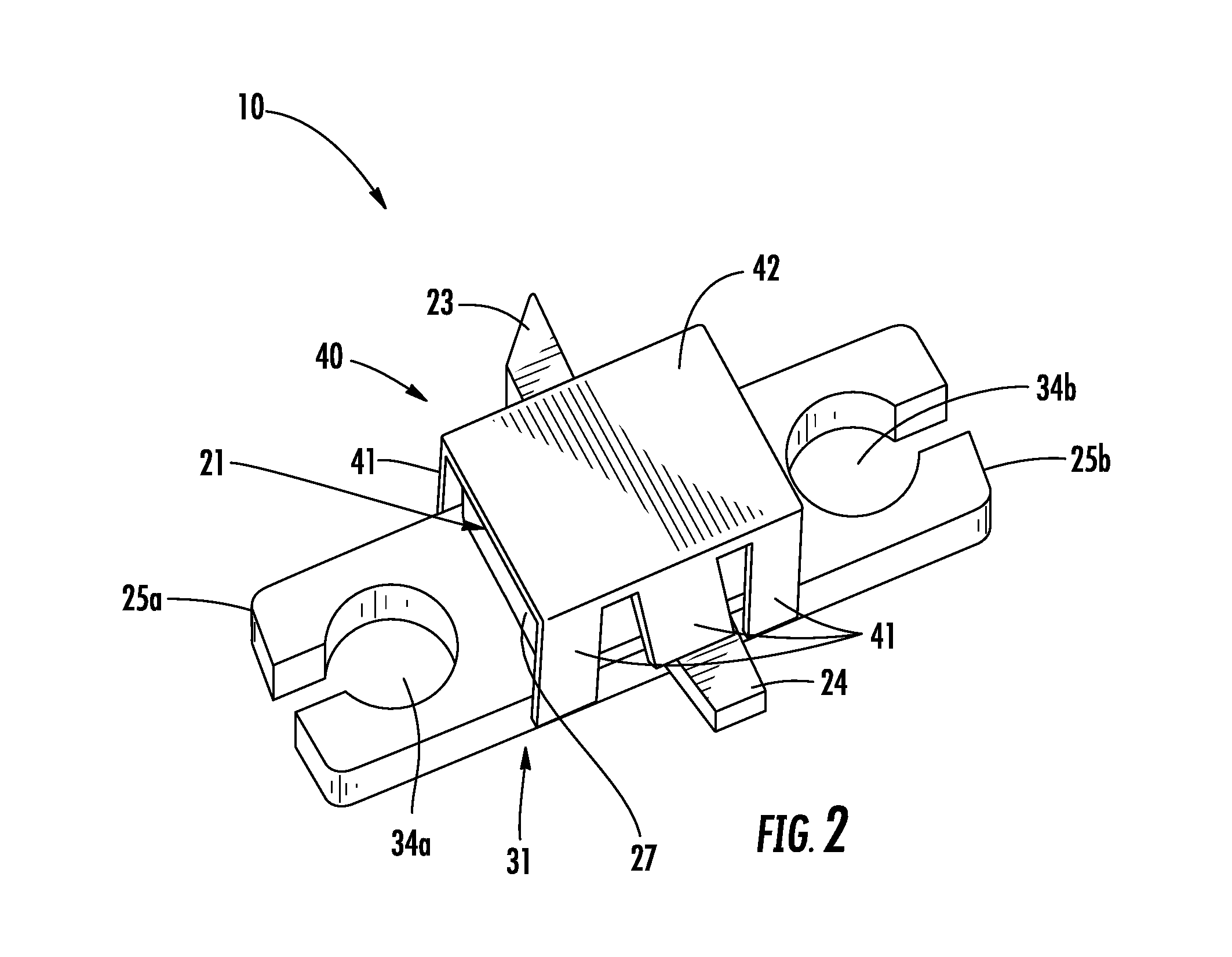
[0018]Referring initially to FIGS. 1 and 2, an electronic device 10 illustratively includes a transistor device 20. The transistor device 20 includes a transistor package 21 and a first conduction terminal, for example, a source terminal, at a bottom surface of the transistor package in the form of the mounting flange 31. The mounting flange 31 has opposing first and second...


PUM


Abstract

An electronic device may include a transistor device including a transistor package and transistor terminals extending outwardly therefrom. The electronic device may also include an electrically conductive body removably coupled to and shorting together the transistor terminals for electrostatic discharge (ESD) protection.

Description

FIELD OF THE INVENTION[0001]The present invention relates to the field of electronics devices and, more particularly, to electrostatic discharge (ESD) protection devices and related methods.BACKGROUND OF THE INVENTION[0002]Some types of electronic devices may be relatively sensitive to electrostatic discharge (ESD). In particular, transistor devices, for example, a radio frequency (RF) power transistor, may be increasingly sensitive to ESD. An ESD as low as 250 volts may destroy the transistor device or damage the transistor device so that is fails.[0003]A transistor device may be most susceptible to ESD damage during handling, which may include, for example, packaging by the manufacturer, removal from the manufacturer's packaging, and / or installation in a an electronic circuit. A transistor device may be most susceptible to damage from gate-to-source and drain-to-source potentials, for example. Typically gate structures may be are most sensitive to ESD.[0004]Several techniques for ...

Claims


Application Information

Patent Timeline
Patent Type & Authority Patents(United States)
IPC IPC(8): H01L21/50H01L27/04
CPCH01L2924/0002H01L23/60H01L2924/00
Inventor MCINTYRE, JOHN ROBERTMUI, ANDREW
Owner HARRIS GLOBAL COMM INC
Why Eureka
Try Eureka