Semiconductor device with leadframe configured to facilitate reduced burr formation

Active Publication Date: 2017-07-11
AMKOR TECH SINGAPORE HLDG PTE LTD
View PDF541 Cites 7 Cited by
  • Summary
  • Abstract
  • Description
  • Claims
  • Application Information

AI Technical Summary

Benefits of technology

The present invention provides an improved semiconductor device package technology that reduces burr formation on the individual leads caused by a saw singulation process used to complete the fabrication of the semiconductor device. This is achieved by arranging and partially etching the leadframe in a way that facilitates a reduction in burr formation, which can cause electrical shorting between certain leads. The invention also eliminates the need for post-treatment to remove the burrs, reducing manufacturing costs and improving reliability.

Problems solved by technology

However, such sawing or punching process often results in undesirable burr formation on the individual leads of each semiconductor device.
However, the need to complete such post-treatment process increases the manufacturing cost, and may further degrade the reliability of the device.

Method used


Image

  • Semiconductor device with leadframe configured to facilitate reduced burr formation
  • Semiconductor device with leadframe configured to facilitate reduced burr formation
  • Semiconductor device with leadframe configured to facilitate reduced burr formation

Examples


Embodiment Construction

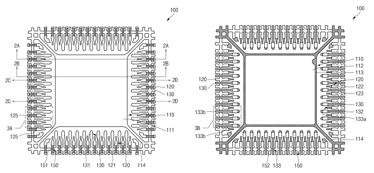
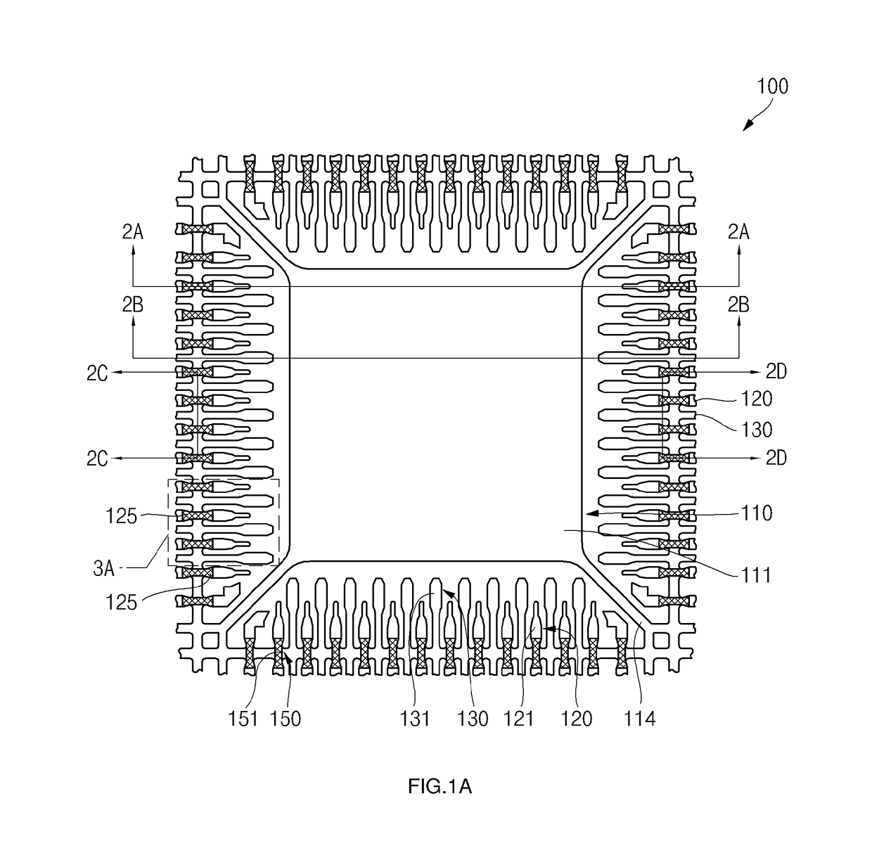
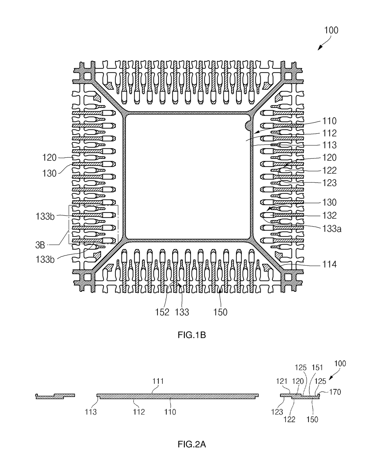
[0024]Referring now to the drawings wherein the showings are for purposes of illustrating preferred embodiments of the present invention only, and not for purposes of limiting the same, FIGS. 4A and 4B depict a semiconductor package or device 200 constructed in accordance with the present invention. The leadframe 100 integrated into the semiconductor package 200 is shown in its unsingulated state in FIGS. 1A and 1B.

[0025]Referring now to FIGS. 1A-1B, 2A-2D, and 3A-3B, the leadframe 100 comprises a generally quadrangular (e.g., square) die paddle or die pad 110 which defines four peripheral edge segments. Additionally, the die pad 110 defines opposed, generally planar top and bottom surfaces 111, 112. As seen in FIGS. 2A and 2B, the die pad 110 of the leadframe 100 is not of uniform thickness. Rather, a peripheral portion of the bottom surface 112 of the die pad 110 is partially etched (e.g., half-etched) to define an etched surface 113. More particularly, the etched surface 113, whi...


PUM


Abstract

A semiconductor package or device including a uniquely configured leadframe defining a plurality of leads which are arranged and partially etched in a manner facilitating a substantial reduction in burr formation resulting from a saw singulation process used to complete the fabrication of the semiconductor device. The semiconductor device includes a die pad defining multiple peripheral edge segments. In addition, the semiconductor device includes a plurality of leads which are provided in a prescribed arrangement. Connected to the top surface of the die pad is at least one semiconductor die which is electrically connected to at least some of the leads. At least portions of the die pad, the leads, the lands, and the semiconductor die are encapsulated by the package body, with at least portions of the bottom surfaces of the die pad and the leads being exposed in a common exterior surface of the package body.

Description

CROSS-REFERENCE TO RELATED APPLICATIONS[0001]Not ApplicableSTATEMENT RE: FEDERALLY SPONSORED RESEARCH / DEVELOPMENT[0002]Not ApplicableBACKGROUND OF THE INVENTION[0003]1. Field of the Invention[0004]The present invention relates generally to integrated circuit package technology and, more particularly, to an increased capacity semiconductor device or package which includes a leadframe defining a plurality of leads which are arranged and partially etched in a manner facilitating a substantial reduction in burr formation resulting from a saw singulation process used to complete the fabrication of the semiconductor device.[0005]2. Description of the Related Art[0006]Semiconductor dies are conventionally enclosed in plastic packages that provide protection from hostile environments and enable electrical interconnection between the semiconductor die and an underlying substrate such as a printed circuit board (PCB) or motherboard. The elements of such a package include a metal leadframe, an...

Claims


Application Information

Patent Timeline
IPC IPC(8): H01L23/495H01L21/48H01L23/00H01L23/31H01L21/56
CPCH01L21/4842H01L23/3107H01L23/49548H01L24/49H01L21/561H01L2224/32245H01L2224/48091H01L2224/48247H01L2224/48465H01L2224/49433H01L2224/73265H01L2224/92247H01L2924/01027H01L2924/01029H01L2924/01047H01L2924/01078H01L2924/01082H01L2924/14H01L2924/19041H01L2924/19043H01L24/73H01L2224/05554H01L2924/181H01L2924/00014H01L2924/351H01L2924/15747H01L2924/014H01L2924/01033H01L24/48H01L2924/00012H01L2924/00H01L2224/45099H01L2224/05599H01L2224/45124H01L2224/45139H01L2224/45144H01L2224/45147H01L2224/49173H01L21/4828H01L23/49541H01L2924/18301H01L23/3157H01L23/4951H01L23/4952
Inventor KIM, HYUN JUNCHUNG, HYUNG KOOKKIM, HONG BAE
Owner AMKOR TECH SINGAPORE HLDG PTE LTD
Why Eureka
Try Eureka