Silicon carbide semiconductor device, method of manufacturing silicon carbide semiconductor device and method of designing silicon carbide semiconductor device

a semiconductor device and silicon carbide technology, applied in the direction of semiconductor devices, basic electric elements, electrical equipment, etc., can solve the problems of reducing the voltage of the protection trench, affecting the electrical field, so as to improve the electrical field and improve the avalanche resistance

Active Publication Date: 2017-07-25
SHINDENGEN ELECTRIC MFG CO LTD
View PDF16 Cites 0 Cited by
  • Summary
  • Abstract
  • Description
  • Claims
  • Application Information

AI Technical Summary

Benefits of technology

[0061]According to the present invention, the horizontal distance between the cell-region linear trench sections is greater than the maximum horizontal distance between sections of the protection trench included in the gate region. Therefore, a higher electrical field is concentrated between the cell-region linear trench sections during reverse biasing. However, since the cell-region linear trench sections occupy a larger area in plan view, even if a high voltage is applied during reverse biasing, the energy is distributed over the larger area occupied by the cell-region linear trench sections. Therefore, according to the present invention, even if the silicon carbide semiconductor device made of silicon carbide adopts a protection trench, an electrical field can be prevented from being locally excessively concentrated during reverse biasing, and the avalanche resistance can be improved.

Problems solved by technology

A silicon carbide semiconductor device made of silicon carbide, such as a SiC-MOSFET, has a high breakdown voltage, so that the gate trench can be insufficient to prevent the electrical field from excessively concentrated in the gate oxide film during reverse biasing, and the gate oxide film can break.
However, such a protection trench can fail to prevent an electrical field from being locally excessively concentrated during reverse biasing because of the interval between sections of the protection trench or the shape of the protection trench in plan view (in the horizontal direction), for example.
If an electrical field is locally excessively concentrated in the protection trench, the withstand voltage of the protection trench decreases, and a desired withstand voltage cannot be achieved.
In addition, if there is a part that has a low withstand voltage, a problem arises in that the avalanche resistance decreases.

Method used


Image

  • Silicon carbide semiconductor device, method of manufacturing silicon carbide semiconductor device and method of designing silicon carbide semiconductor device
  • Silicon carbide semiconductor device, method of manufacturing silicon carbide semiconductor device and method of designing silicon carbide semiconductor device
  • Silicon carbide semiconductor device, method of manufacturing silicon carbide semiconductor device and method of designing silicon carbide semiconductor device

Examples


first embodiment

>

[0069]In the following, a silicon carbide semiconductor device, a method of manufacturing the silicon carbide semiconductor device and a method of designing the silicon carbide semiconductor device according to a first embodiment of the present invention will be described with reference to the drawings.

[0070]The silicon carbide semiconductor device according to this embodiment is a trench-structure MOSFET, for example. In the following, the silicon carbide semiconductor device will be described as the trench-structure MOSFET. However, the trench-structure MOSFET is only an example of the silicon carbide semiconductor device, and the present invention can be applied to other devices structures having a MOS gate, such as an insulated gate bipolar transistor (IGBT).

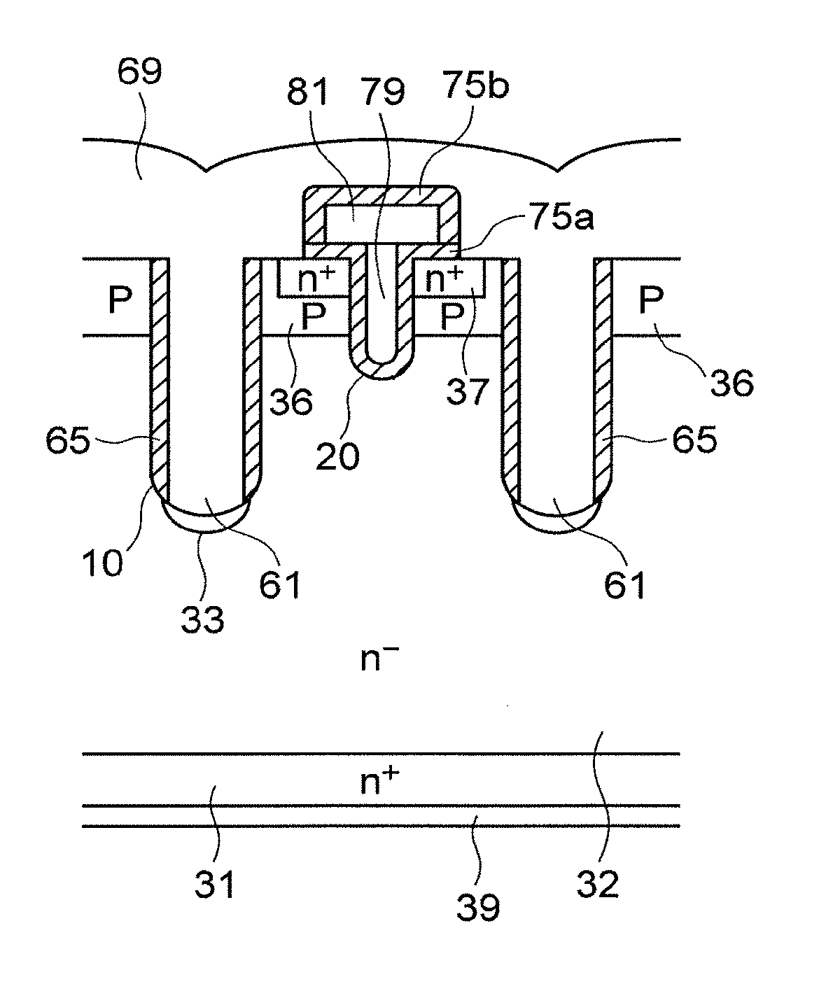
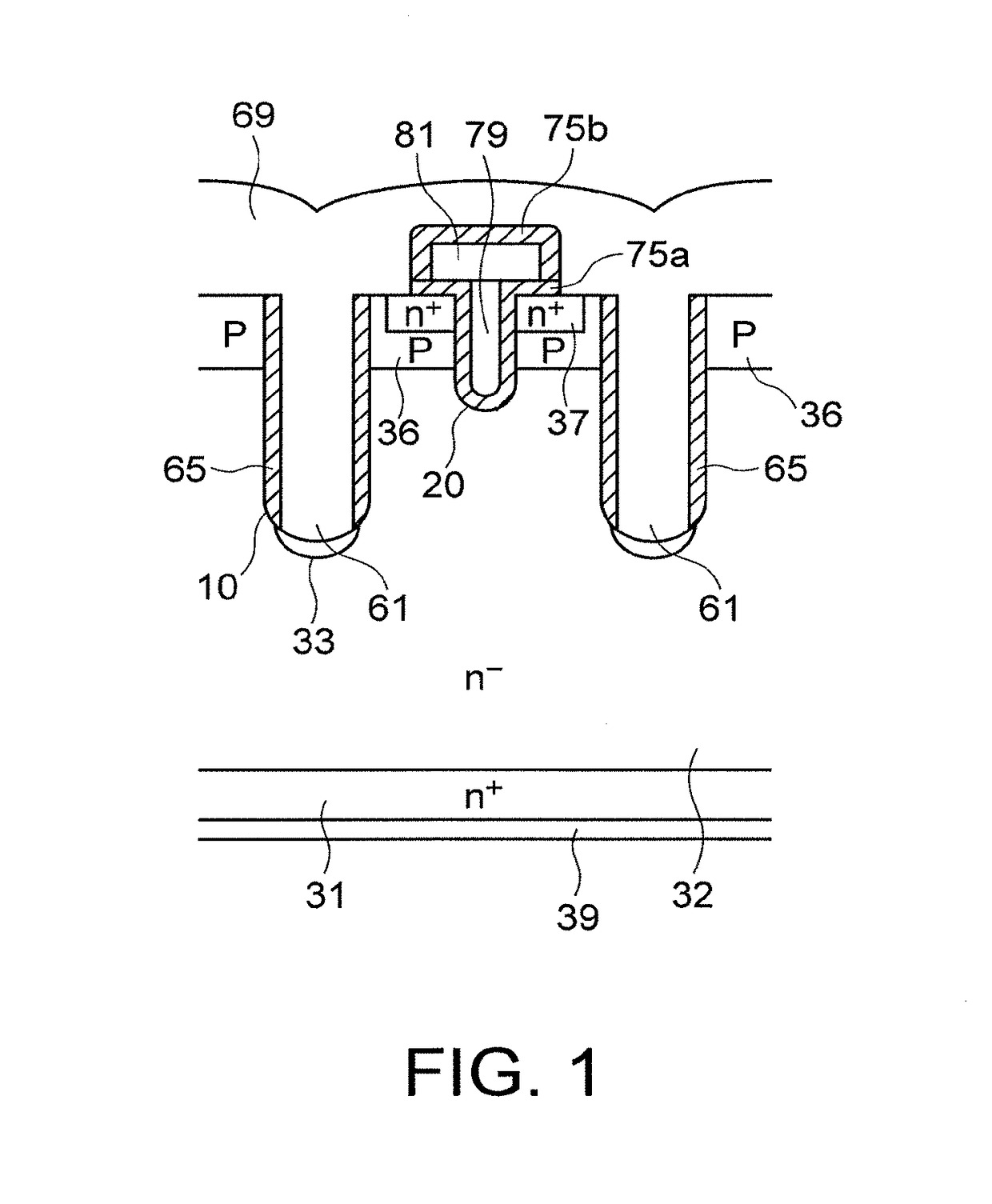
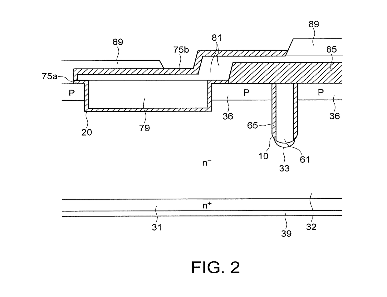
[0071]As shown in FIG. 1, the silicon carbide semiconductor device according to this embodiment includes an n-type silicon carbide semiconductor substrate 31 of high concentration (a silicon carbide semiconductor substrate ...

second embodiment

[0115]Next, a second embodiment of the present invention will be described. FIG. 7, which is used in the description of this embodiment, is an enlarged top view of a guard ring of a silicon carbide semiconductor device according to this embodiment and a vicinity thereof. Specifically, FIG. 7 is a top view of the part “A2” in FIG. 4.

[0116]According to the first embodiment, the protection trench 10 included in the gate region has three or more gate-region linear trench sections 16 that extend straight in the horizontal direction, although no mention has been made as to the relationship between the gate-region linear trench sections 16 and the guard ring 80. In this respect, according to the second embodiment, three or more gate-region linear trench sections 16 are provided adjacent to a part of the guard ring 80 and in parallel with the guard ring 80. And a horizontal distance “d1” between the gate-region linear trench section 16a adjacent to the guard ring 80 and the gate-region line...


PUM

PropertyMeasurementUnit
conductivityaaaaaaaaaa
conductivity typeaaaaaaaaaa
depthaaaaaaaaaa

Abstract

A silicon carbide semiconductor device includes a silicon carbide layer 32 of a first conductivity type, a silicon carbide layer 36 of a second conductivity type, a gate trench 20, a gate electrode 79 provided in the gate trench 20, and a protection trench 10 formed to a depth greater than the gate trench 20. A region in the horizontal direction that includes both the gate trench 20 and a protection trench 10 that surrounds the gate trench 20 with at least a part of the gate trench 20 left unenclosed is a cell region, and a region in the horizontal direction that includes a protection trench 10 and in which a gate pad 89 or a lead electrode connected to the gate pad is disposed is a gate region.

Description

CROSS-REFERENCE TO RELATED APPLICATION(S)[0001]This application is the U.S. National Stage of International Patent Application No. PCT / JP2014 / 075192 filed on Sep. 24, 2014, the disclosure of which is incorporated in its entirety herein by reference.TECHNICAL FIELD[0002]The present invention relates to a silicon carbide semiconductor device, which is made of silicon carbide, a method of manufacturing the silicon carbide semiconductor device, and a method of designing the silicon carbide semiconductor device.BACKGROUND ART[0003]There are known conventional semiconductor devices made of silicon, such as a trench-type Si-MOSFET. Japanese Patent Laid-Open No. 06-132539 discloses a semiconductor device having a vertical insulated gate bipolar transistor that includes a semiconductor substrate of a first conductivity type, a first semiconductor layer of the first conductivity type of low impurity concentration formed on the principal surface of the semiconductor substrate, a second semicon...

Claims


Application Information

Patent Timeline
Patent Type & Authority Patents(United States)
IPC IPC(8): H01L29/78H01L29/06H01L29/40H01L29/16H01L29/423H01L29/66
CPCH01L29/407H01L29/4238H01L29/66068H01L29/7811H01L29/7813H01L29/0619H01L29/0623H01L29/0696H01L29/1608H01L29/404H01L29/7397
Inventor INOUE, TETSUTOSUGAI, AKIHIKONAKAMURA, SHUNICHI
Owner SHINDENGEN ELECTRIC MFG CO LTD
Why Eureka
Try Eureka