
Thermosetting adhesive sheet and semiconductor device manufacturing method

a technology of adhesive sheet and semiconductor device, which is applied in the direction of semiconductor device, semiconductor/solid-state device details, electrical apparatus, etc., can solve the problems of reduced transparency, high defect rate, and significant stress of semiconductor wafers, and achieve excellent laser mark visibility and alignment mark readability, and high-quality semiconductor devices

Active Publication Date: 2017-09-05
DEXERIALS CORP
View PDF5 Cites 0 Cited by
  • Summary
  • Abstract
  • Description
  • Claims
  • Application Information

AI Technical Summary

Benefits of technology

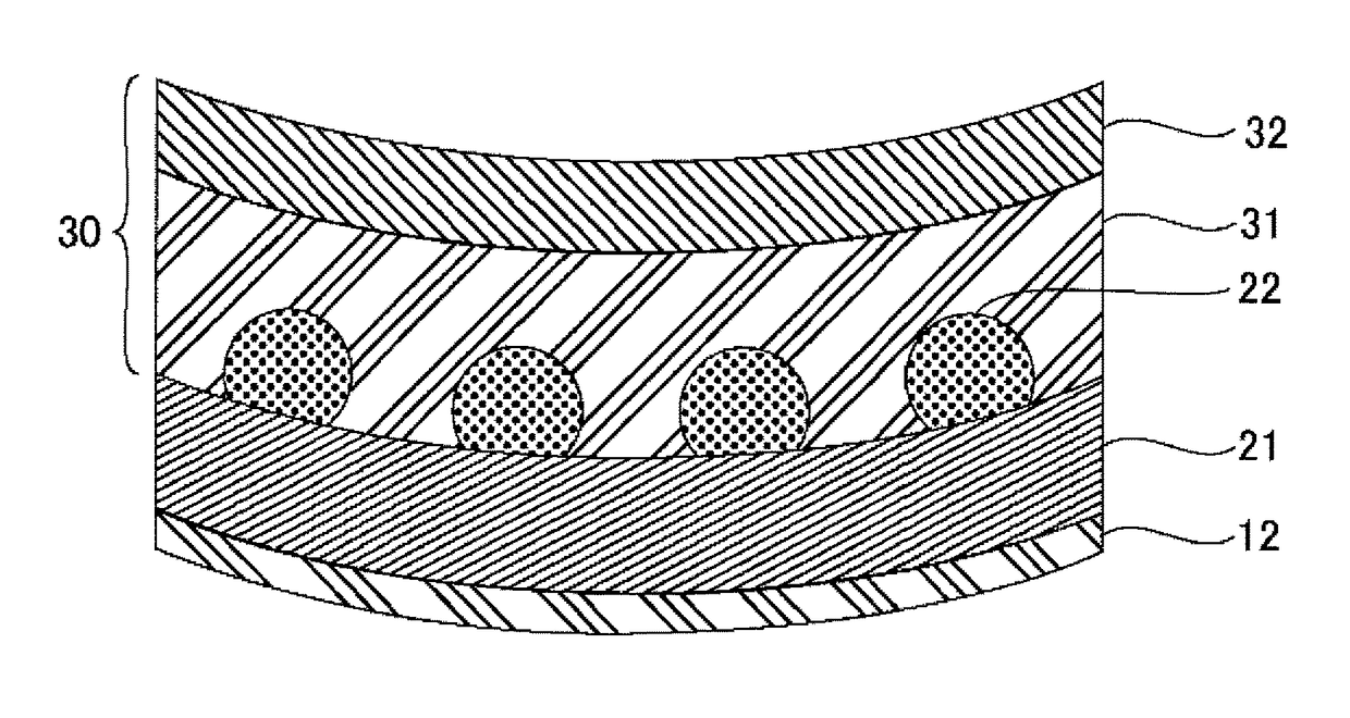
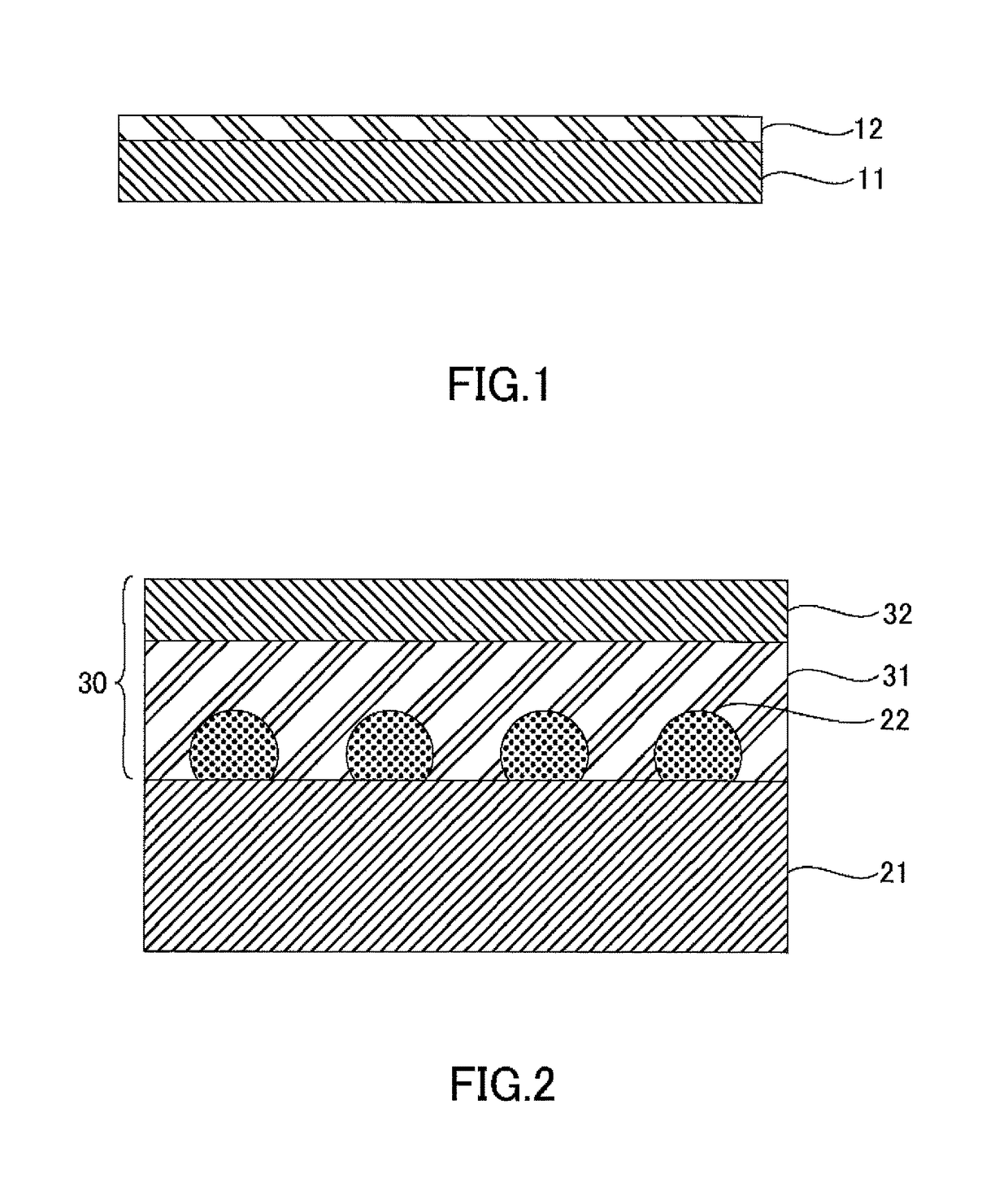
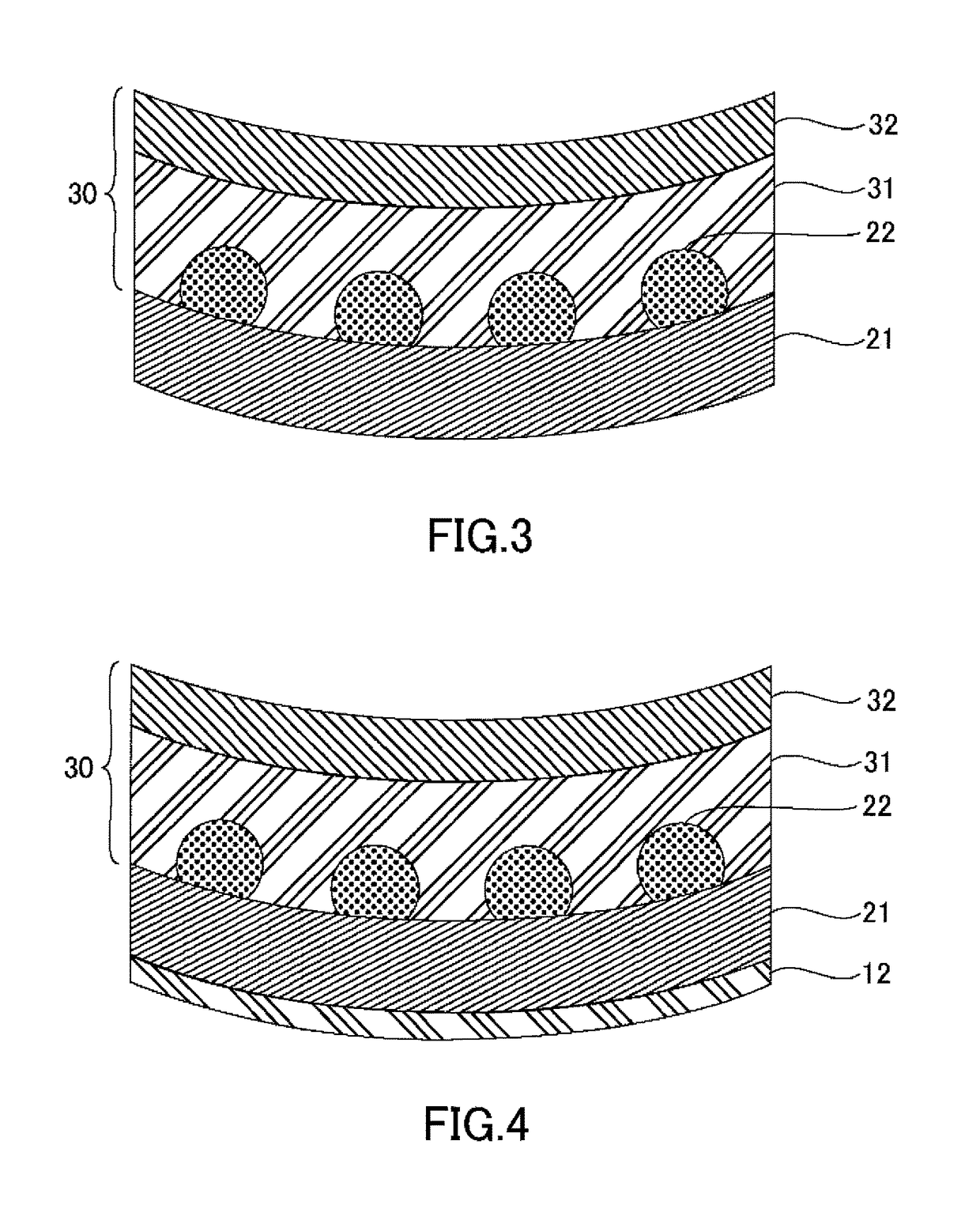
[0010]The thermosetting adhesive sheet according to the present disclosure is able to achieve excellent laser mark visibility and alignment mark readability by including a predetermined amount of the transparent filler and the colorant. A high-quality semiconductor device can thus be achieved by using the thermosetting adhesive sheet according to the present disclosure.

Problems solved by technology

In manufacturing processes of semiconductor chips, dicing (individualization) processes cause significant stress in semiconductor wafers.
Microcracks have thus occurred in semiconductor wafers which have led to high defect rates.
However, to improve laser mark readability, in the case of adding a coloring agent to the thermosetting adhesive sheet, transparency is reduced and alignment mark readability might be problematic.

Method used


Image

  • Thermosetting adhesive sheet and semiconductor device manufacturing method
  • Thermosetting adhesive sheet and semiconductor device manufacturing method
  • Thermosetting adhesive sheet and semiconductor device manufacturing method

Examples


examples

[0090]3. Examples

[0091]Examples according to the present disclosure will now be described.

[0092]3.1 First Examples

[0093]In the first examples, thermosetting adhesive sheets were manufactured and laser mark visibility and alignment mark readability were evaluated.

[0094]Thermosetting Adhesive Sheet Manufacture

[0095]The constituents listed below were blended to prepare resin compositions. These were then applied to release-treated PET (polyethylene terephthalate) by using a bar coater which was then dried in an oven at 80° C. for 3 minutes to manufacture thermosetting adhesive sheets having a thickness of 20 μm (cover release-treated PET (25 μm)) / thermosetting adhesive sheet (20 μm) / base release-treated PET (50 μm).

[0096]FX293: fluorene-type phenoxy resin (manufactured by NIPPON STEEL & SUMIKIN CHEMICAL CO., LTD.)

[0097]SG-80H: acrylic elastomer (manufactured by Nagase ChemteX Corporation)

[0098]4-HBA: 4-hydroxy-butyl acrylate (manufactured by SHIN-NAKAMURA CHEMICAL CO, LTD., (meth)acryl...

example 1

[0111]A thermosetting binder was prepared having 5 pts. mass of a fluorene-type phenoxy resin (FX293), 20 pts. mass of an acrylic-type elastomer (SG-80H), 50 pts. mass of a monofunctional acrylate (4-HBA) and 5 pts. mass of an organic peroxide (PEROYL L). To 80 pts. mass of this thermosetting binder, 50 pts. mass of silica (primary particle diameter: 100 nm), 0.5 pts. mass of carbon black and 2 pts. mass of an acrylic-type coupling agent (KBM-5103) were blended and thermosetting adhesive sheets were manufactured.

[0112]As represented in Table 1, transmittance of the thermosetting adhesive sheets for a wavelength of 1000 nm was 50%. Moreover, the laser mark visibility evaluation was G and the alignment mark readability evaluation was VG.

example 2

[0113]A thermosetting binder was prepared having 5 pts. mass of a fluorene-type phenoxy resin (FX293), 20 pts. mass of an acrylic-type elastomer (SG-80H), 50 pts. mass of an alicyclic epoxy resin (CEL-2021) and 5 pts. mass of a phenol novolac (TD-2131) as a curing agent. To 80 pts. mass of this thermosetting binder, 5 pts. mass of a DBU-type tetraphenylborate salt (U-CAT 5002) as an auxiliary curing agent, 50 pts. mass of silica (primary particle diameter: 100 nm), 0.5 pts. mass of carbon black and 2 pts. mass of an acrylic-type coupling agent (KBM-403) were blended and thermosetting adhesive sheets were manufactured.

[0114]As represented in Table 1, transmittance of the thermosetting adhesive sheets for a wavelength of 1000 nm was 50%. Moreover, the laser mark visibility evaluation was G and the alignment mark readability evaluation was VG.


PUM

PropertyMeasurementUnit
average primary particle diameteraaaaaaaaaa
one-minute half-life temperatureaaaaaaaaaa
average primary particle diameteraaaaaaaaaa

Abstract

A thermosetting adhesive sheet comprises a thermosetting binder, a transparent filler having an average primary particle diameter from 1 nm to 1000 nm and a colorant; wherein content of the transparent filler is from 30 to 100 pts. mass with respect to 80 pts. mass of the thermosetting binder and content of the colorant is from 0.5 to 3.0 pts. mass with respect to 80 pts. mass of the thermosetting binder; this thermosetting adhesive sheet is applied to a grinding-side surface of a semiconductor wafer and before dicing the semiconductor wafer. Printing using laser marking is thus made clear enabling excellent laser mark visibility and accurate alignment using infrared light.

Description

TECHNICAL FIELD[0001]The present disclosure relates to a thermosetting adhesive sheet which reinforces a semiconductor wafer and a method for manufacturing a semiconductor device in order to prevent cracks during a dicing step.BACKGROUND ART[0002]In manufacturing processes of semiconductor chips, dicing (individualization) processes cause significant stress in semiconductor wafers. Microcracks have thus occurred in semiconductor wafers which have led to high defect rates.[0003]In order to prevent such a problem, applying a thermosetting adhesive sheet immediately before dicing (after backgrinding) to reinforce the semiconductor wafer has been proposed (for example, refer to PLT 1).[0004]Furthermore, in order to ensure traceability for quality of semiconductor chips, it is desirable to laser-mark information such as a lot number on the thermosetting adhesive sheet. Still further, to enable accurate alignment, it is desirable to read alignment marks on the back surface of the semicond...

Claims


Application Information

Patent Timeline
Patent Type & Authority Patents(United States)
IPC IPC(8): H01L21/683H01L21/78H01L23/00H01L23/544H01L23/31
CPCH01L23/562H01L21/6836H01L21/78H01L2224/11H01L23/3114H01L23/3157H01L23/544H01L2221/6834H01L2221/68327H01L2221/68336H01L2223/54426H01L2223/54433H01L2223/54486H01L2224/13111H01L21/304H01L2924/01047H01L2924/014H01L2924/01029C09J7/20H01L21/30625H01L21/324H01L24/28H01L24/31C09J2203/326
Inventor MORI, DAICHI
Owner DEXERIALS CORP
Learn More