
Method of manufacturing semiconductor device and method of forming pattern

a semiconductor device and pattern technology, applied in the direction of semiconductor devices, photomechanical devices, instruments, etc., can solve the problems of high manufacturing cost, inability to form fine resist patterns, and inability to achieve high-performance and accurate patterning of surface layers, etc., to achieve convenient, high-quality, easy-to-use results

Active Publication Date: 2006-06-13
FUJITSU SEMICON LTD
View PDF10 Cites 1 Cited by
  • Summary
  • Abstract
  • Description
  • Claims
  • Application Information

AI Technical Summary

Benefits of technology

[0011]An object of the present invention is to provide a method of manufacturing a semiconductor device and a method of forming a pattern which can, conveniently, easily and highly accurately, form a fine pattern of a high aspect ratio.
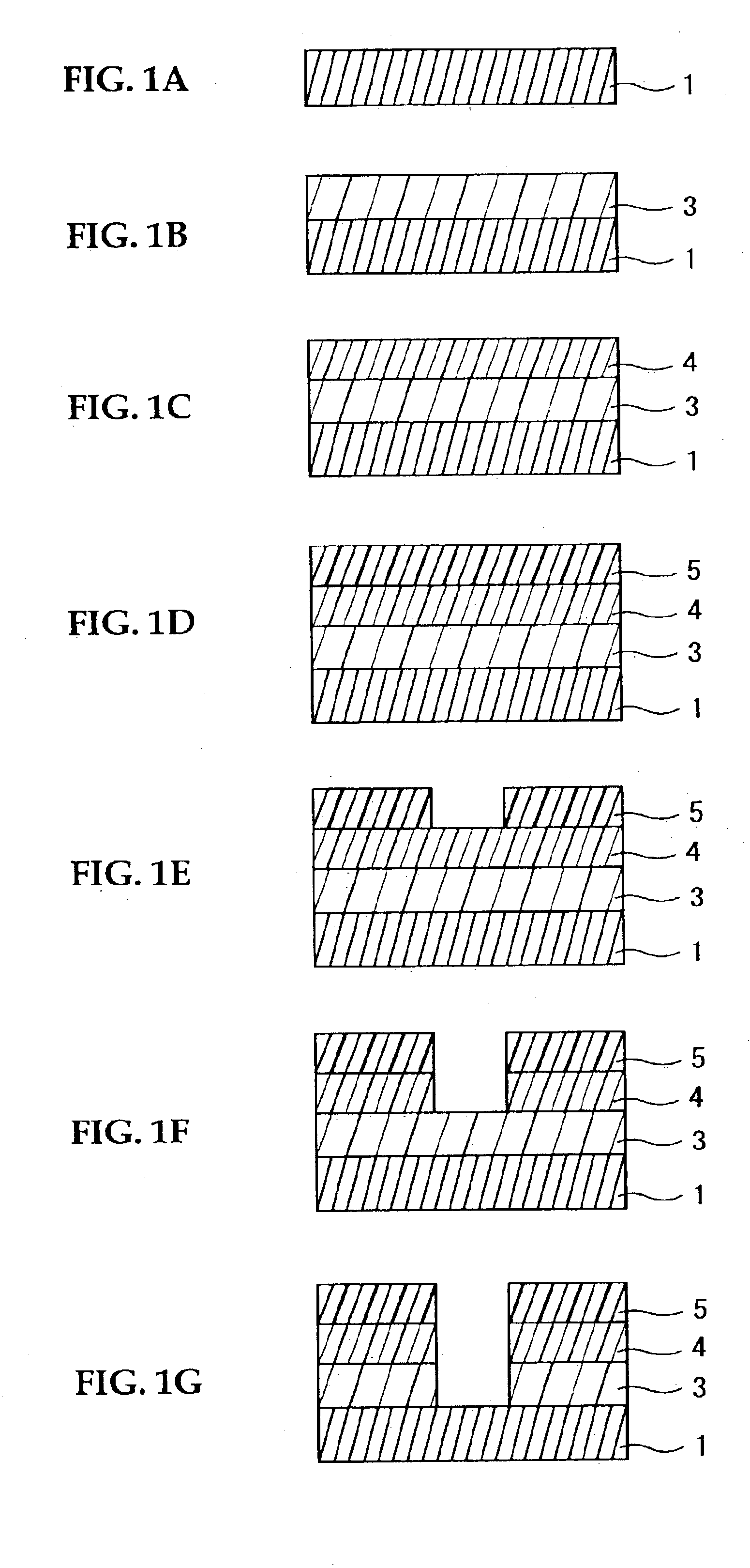
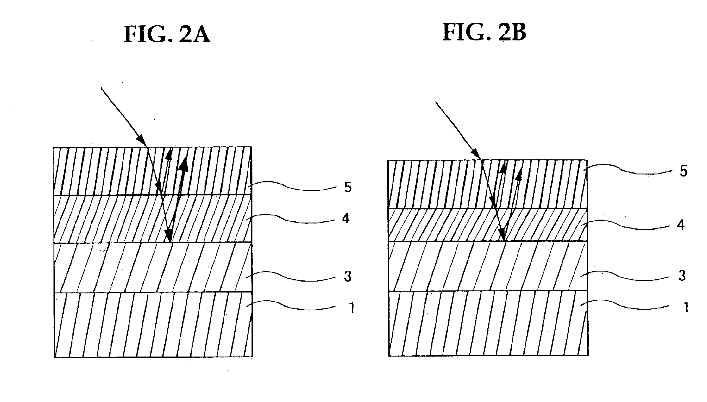
[0013]A method of manufacturing a semiconductor device and a method of forming a pattern, according to a second aspect of the present invention comprises the step of forming a laminated film for pattern formation on a substrate, in which the laminated film for pattern formation includes an innermost layer (lower layer), an inner layer (intermediate layer) and a surface layer (upper layer), an extinction coefficient k of the innermost layer is less than 0.3, and an extinction coefficient k of the inner layer is 0.18 or more. In the second aspect, the innermost layer is light transmitting, and the inner layer is light absorbent and has low reflectance. Thus, reflection of the exposure light used in patterning the surface layer is effectively suppressed, and multiple interference of the reflected light does not occur. Thus, an increase in the dispersion of the line widths of the surface layer (upper layer) due to variations in the thickness of the inner layer is suppressed. As a result, a fine pattern having a high aspect ratio is formed accurately and conveniently. Fine wires or the like can be worked by using the fine pattern, and a high-quality semiconductor device is manufactured.

Problems solved by technology

However, with a substrate having large steps, it is not possible to form a fine resist pattern.
A problem arises in that high-performance and accurate patterning of the surface layer cannot be carried out due to the interference of the light reflected by the innermost layer.
However, in these cases, problems arise in that the manufacturing costs are high, and the like (refer to, for example, JP-A No. 60-254034 and JP-A No. 05-265224).
In a case in which the inner layer (intermediate layer) is formed to be thick, a problem arises in that even the inner layer (intermediate layer) is affected and deteriorates when the surface layer (upper layer) is damaged and the configuration thereof deteriorates.
On the other hand, when the inner layer (intermediate layer) is formed to be thin, it is easy for defects to arise at the inner layer (intermediate layer).
For example, when the innermost layer (lower layer) is formed of a resin which contains an additive, a problem arises in that it is easy for pin holes to arise in the mask patterned formed by the inner layer (intermediate layer).
When etching of the innermost layer (lower layer) is carried out by using a mask pattern in which pin holes have arisen, defects caused by the pin holes arise in the formed pattern of the innermost layer (lower layer), and there is the problem that it is not possible to carry out high-performance and accurate patterning.

Method used


Image

  • Method of manufacturing semiconductor device and method of forming pattern
  • Method of manufacturing semiconductor device and method of forming pattern
  • Method of manufacturing semiconductor device and method of forming pattern

Examples


experiment 1

(Pattern Formation)

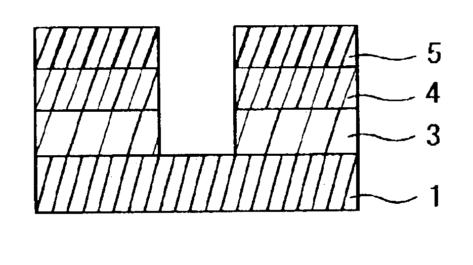
[0104]Referring into FIG. 7, a resist for the innermost layer (PFI-37M, manufactured by Sumitomo Chemical Co., Ltd.) was coated to a thickness of 300 nm on a substrate 1 to be worked. Thereafter, baking was carried out for 60 seconds at 200° C., and the innermost layer (lower layer) 3 was thus formed. Note that the extinction coefficient k of the innermost layer (lower layer) 3 was 0.54. Next, a composition for inner layer formation was coated to have a thickness of 85 nm (0.085 μm) on the innermost layer (lower layer) 3. Baking was carried out for 60 seconds at 200° C., and the inner layer (intermediate layer) 4 was thus formed on the innermost layer (lower layer) 3. The composition for inner layer formation was a solution in which the polysiloxane compound expressed by following Formula (4) was dissolved in methyl amyl ketone (MAK). The extinction coefficient k of the inner layer (intermediate layer) 4 was 0.36. Note that error of the measurement of the extincti...

experiment 2

(Pattern Formation)

[0108]An accurate and fine hole pattern such as that of Experiment 1 was formed in the same way as in Experiment 1, except that the resist for the innermost layer (PFI-37M, manufactured by Sumitomo Chemical Co., Ltd.) was replaced with adamantyl methacrylate, 4,4-diazidochalcone, and propylene glycol monomethyl acetate (PGMEA) was used as the solvent, and the extinction coefficient k of the innermost layer (lower layer) was changed from 0.36 to 0.45 (innermost Layer (lower layer) is Not Light Absorbent).

[0109]As shown in FIG. 8, it is clear from Experiments 1 and 2 that when the inner layer (intermediate layer) is formed by using a polyorganosiloxane compound (which has a light absorbent group) expressed by the above Formula (4), the inner layer (intermediate layer) is light absorbent and has low reflectance, and in this case, it is therefore clear that the patterning accuracy improves and there is little dispersion in thickness (the dimensional uniformity improve...

experiment 3

(Experiment 3)

[0111]As shown in FIG. 10A, an insulating film 2, which served as an object to be worked and which was prepared by baking an organic film, was formed on an Si wafer 1 serving as a substrate. Composition A for innermost layer formation, which served as the material for an innermost layer (lower layer) 3 and which was prepared by dissolving a novolak resin in a solvent and adding a surfactant as an additive, was coated by the spin coating method on the insulating film 2. Thereafter, pre-baking was carried out for 60 seconds at 200° C. Thereafter, baking was carried out for, 60 seconds at 350° C., and the innermost layer (lower layer) 3 having a thickness of 85 nm was formed on the insulating film 2. Note that the extinction coefficient k of the innermost layer (lower layer) 3 was 0.54 (the innermost layer (lower layer) 3 was light absorbent).

[0112]Next, as shown in FIG. 10B, an organic precursor substance (siloxane A) serving as a material for inner layer formation was c...


PUM


Abstract

The present invention provides a method of manufacturing a semiconductor device which includes a step of forming a laminated film for pattern formation on a substrate, in which the laminated film for pattern formation includes an innermost layer, an inner layer and a surface layer, an extinction coefficient k of the innermost layer is 0.3 or more, and an extinction coefficient k of the inner layer is 0.12 or more. It also provides a method of forming a pattern which includes a step of forming a laminated film for pattern formation on a substrate, in which the laminated film for pattern formation includes an innermost layer, an inner layer and a surface layer, an extinction coefficient k of the innermost layer is 0.3 or more, and an extinction coefficient k of the inner layer is 0.12 or more.

Description

CROSS-REFERENCE TO RELATED APPLICATIONS[0001]This application is based upon and claims the benefit of priority from the prior Japanese Patent Application No. 2002-190666 filed on Jun. 28, 2002, No. 2002-245798, filed on Aug. 26, 2002, and No. 2003-157397, filed on Jun. 2, 2003, the entire contents of which are incorporated herein by reference.BACKGROUND OF THE INVENTION[0002]1. Field of the Invention[0003]The present invention relates to a method of manufacturing a semiconductor device, which is suited to the formation of wiring patterns and the like in semiconductor devices, and to a method of forming a pattern.[0004]2. Description of the Related Art[0005]In recent years, the trends toward making wires finer, increasing the number of layers, and the like have intensified in the manufacture of semiconductor integrated circuits in order to achieve greater integration, higher speeds, and the like. In semiconductor devices, there has been the trend toward increasing the aspect ratio of...

Claims


Application Information

Patent Timeline
IPC IPC(8): H01L21/31G03F7/075G03F7/09G03F7/11G03F7/26H01L21/027H01L21/033H01L21/312H01L21/768
CPCG03F7/091H01L21/02126H01L21/02216H01L21/02282H01L21/0332H01L21/3122H01L21/76811H01L21/0275G03F7/0757Y10S438/952Y10S438/942G03F7/26
Inventor OTOGURO, AKIHIKOTAKECHI, SATOSHIDEGUCHI, TAKATOSHI
Owner FUJITSU SEMICON LTD
Learn More