

Thermosetting adhesive sheet and semiconductor device manufacturing method
- Summary
- Abstract
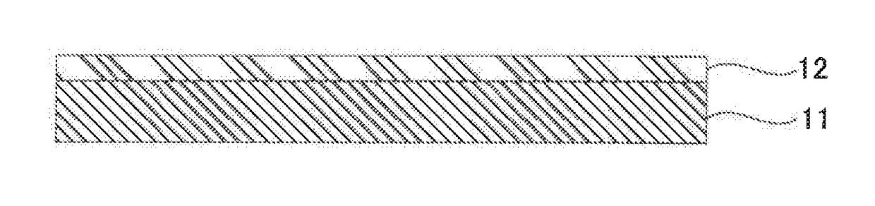
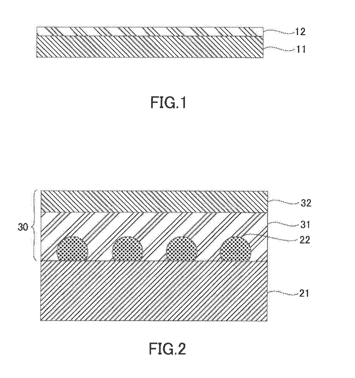
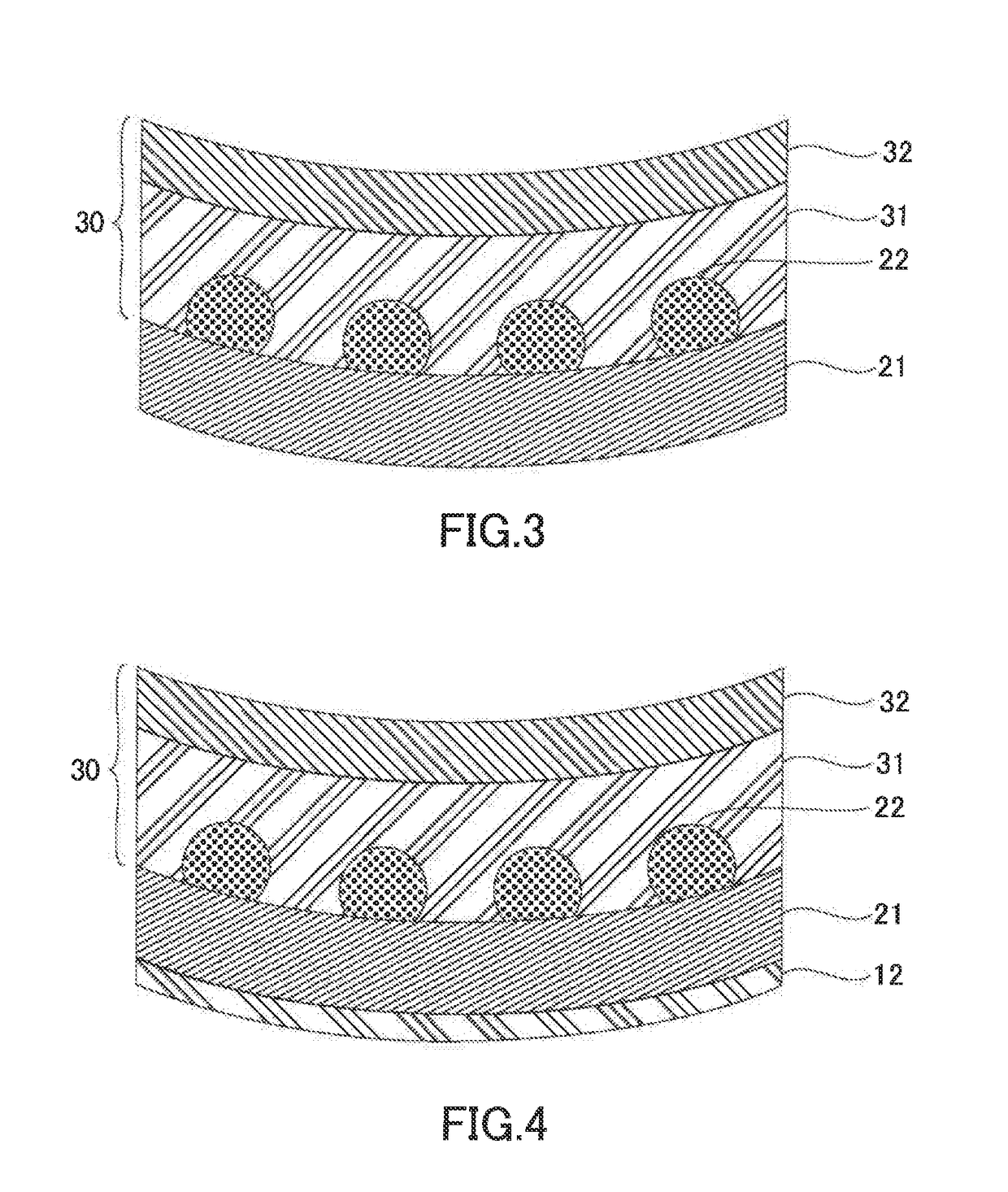
- Description
- Claims
- Application Information
AI Technical Summary
Benefits of technology
Problems solved by technology
Method used
Image

Examples
example 1
[0095]As represented in Table 1, a resin composition was prepared having 100 pts. mass of a resin component containing 39 pts. mass of a solid epoxy compound (jER1009), 60 pts. mass of a curing agent (HX-3941HP), and 1 pts. mass of a coupling agent (A-187), to which 80 pts. mass of silica (Aerosil R202) was added. Moles of epoxy groups for 100 pts. mass of the resin component was 1.368E-04, and blending amount of the filler was 80 pts. mass with respect to 100 pts. mass of the resin component. Thermosetting adhesive sheets prepared using this resin composition were evaluated as A for film-formation properties, B for suppression of chipping during dicing, and B for control of wafer warping.
example 2
[0096]As represented in Table 1, a resin composition was prepared having 100 pts. mass of a resin component containing 38 pts. mass of a solid epoxy compound (jER1009), 59 pts. mass of a curing agent (HX-3941HP), and 1 pts. mass of a coupling agent (A-187), to which 80 pts. mass of silica (Aerosil R202) and 2 pts. mass carbon black was added. Moles of epoxy groups for 100 pts. mass of the resin component was 1.361E-04, and blending amount of the filler was 82 pts. mass with respect to 100 pts. mass of the resin component. Thermosetting adhesive sheets prepared using this resin composition were evaluated as A for film-formation properties, B for suppression of chipping during dicing, and B for control of wafer warping.
example 3
[0097]As represented in Table 1, a resin composition was prepared having 100 pts. mass of a resin component containing 32 pts. mass of a polyfunctional solid epoxy compound (jER1031S), 67 pts. mass of a curing agent (HX-3941HP), and 1 pts. mass of a coupling agent (A-187), to which 80 pts. mass of silica (Aerosil R202) was added. Moles of epoxy groups for 100 pts. mass of the resin component was 1.600E-03, and blending amount of the filler was 80 pts. mass with respect to 100 pts. mass of the resin component. Thermosetting adhesive sheets prepared using this resin composition were evaluated as A for film-formation properties, B for suppression of chipping during dicing, and A for control of wafer warping.
PUM
| Property | Measurement | Unit |
|---|---|---|
| Thickness | aaaaa | aaaaa |
| Mass | aaaaa | aaaaa |
| Content | aaaaa | aaaaa |
Abstract
Description
Claims
Application Information