
Thermosetting adhesive sheet and semiconductor device manufacturing method

a technology of adhesive sheets and semiconductor devices, applied in the direction of film/foil adhesives without carriers, film/foil adhesives, non-macromolecular adhesive additives, etc., can solve the problems of reducing the service life increasing the defect rate, and affecting the application of dicing tapes. , to achieve the effect of reducing the warping of the semiconductor wafer, reducing the chipping, and increasing the flatness of the wafer

Active Publication Date: 2018-11-01
DEXERIALS CORP
View PDF0 Cites 1 Cited by
  • Summary
  • Abstract
  • Description
  • Claims
  • Application Information

AI Technical Summary

Benefits of technology

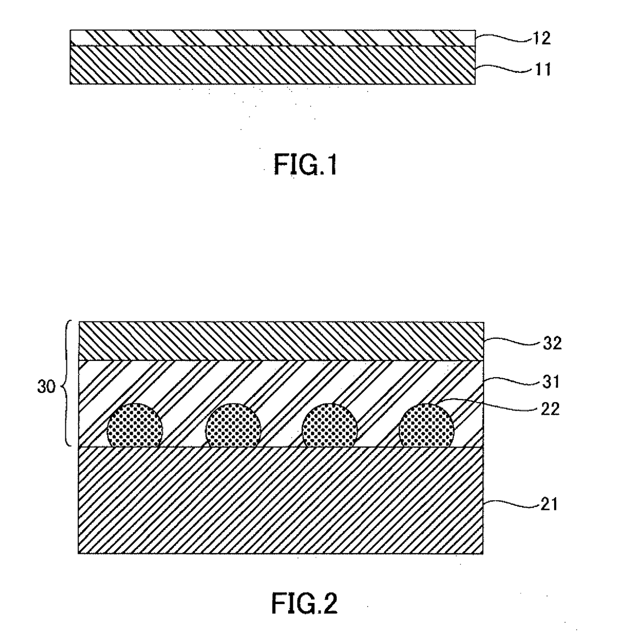
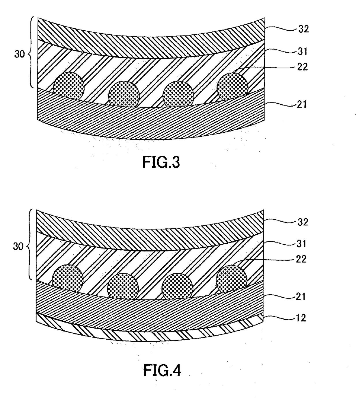
The patent aims to reduce semiconductor wafer warping, which can cause chipping and lower quality semiconductor devices. This is achieved by applying a thermosetting sheet to the ground surface of the wafer and curing it to contract it, resulting in a more flat wafer during dicing.

Problems solved by technology

In manufacturing processes of semiconductor chips, dicing (separation) processes cause significant stresses in semiconductor wafers.
This can cause microcracks in semiconductor wafers and might increase defect rates.
However, thinner semiconductor wafers have increased semiconductor wafer warping, which might impede dicing tape application.

Method used


Image

  • Thermosetting adhesive sheet and semiconductor device manufacturing method
  • Thermosetting adhesive sheet and semiconductor device manufacturing method
  • Thermosetting adhesive sheet and semiconductor device manufacturing method

Examples


example 1

[0105]As represented in Table 1, a resin composition was prepared having 84 pts. mass of a resin component containing 20 pts. mass of a trifunctional acrylate (M-315), 60 pts. mass of a bisphenol A epoxy acrylate (VR-90), 1 pts. mass of a coupling agent (KBM-503), and 3 pts. mass of an organic peroxide (PEROYL L), to which 100 pts. mass of an inorganic filler (Aerosil R202) was added. Blending amount of the inorganic filler was 119 pts. mass with respect to 100 pts. mass of the resin component, content of the solid (meth)acrylate in the resin component was 71 wt %, content of the (meth)acrylate in the resin component was 95 wt %, and the total value obtained by multiplying the number of functional groups per unit molecular weight of the (meth)acrylate by content of the (meth)acrylate in the resin component was 2.99E-03. Thermosetting adhesive sheets prepared using this resin composition were evaluated as PASS for film-formation properties, PASS for suppression of chipping during dic...

example 2

[0106]As represented in table 1, except that 70 pts. mass of the inorganic filler (Aerosil R202) was added, a resin composition was prepared as in example 1. Blending amount of the inorganic filler was 83 pts. mass with respect to 100 pts. mass of the resin component, content of the solid (meth)acrylate in the resin component was 71 wt %, content of (meth)acrylate in the resin component was 95 wt %, and the total value obtained by multiplying the number of functional groups per unit molecular weight of the (meth)acrylate by the content of the (meth)acrylate in the resin component was 2.99E-03. Thermosetting adhesive sheets prepared using this resin composition were evaluated as PASS for film-formation properties, PASS for suppression of chipping during dicing, and A for control of thin wafer warping.

example 3

[0107]As represented in table 1, except that 150 pts. mass of the inorganic filler (Aerosil R202) was added, a resin composition was prepared as in example 1. Blending amount of the inorganic filler was 179 pts. mass with respect to 100 pts. mass of the resin component, content of the solid (meth)acrylate in the resin component was 71 wt %, content of (meth)acrylate in the resin component was 95 wt %, and the total value obtained by multiplying the number of functional groups per unit molecular weight of the (meth)acrylate by the content of the (meth)acrylate in the resin component was 2.99E-03. Thermosetting adhesive sheets prepared using this resin composition were evaluated as PASS for film-formation properties, PASS for suppression of chipping during dicing, and A for control of thin wafer warping.


PUM

PropertyMeasurementUnit
thicknessaaaaaaaaaa
temperatureaaaaaaaaaa
melting pointaaaaaaaaaa

Abstract

Provided are a thermosetting adhesive sheet and a method for manufacturing a semiconductor device capable of reducing semiconductor wafer warping and chipping. The thermosetting adhesive sheet includes a thermosetting adhesive layer containing a resin component and a filler, the resin component containing a (meth)acrylate and a polymerization initiator, the (meth)acrylate containing a solid (meth)acrylate and a trifunctional or higher functional (meth)acrylate, content of the solid (meth)acrylate in the resin component being 55 wt % or more; a total value obtained by multiplying the number of functional groups per unit molecular weight of the (meth)acrylate by content of the (meth)acrylate in the resin component being 2.7E-03 or more, and blending amount of the filler being 80 to 220 pts. mass with respect to 100 pts. mass of the resin component.

Description

TECHNICAL FIELD[0001]The present disclosure relates to a thermosetting adhesive sheet for reinforcing a semiconductor wafer and preventing cracks during a dicing process and a method for manufacturing a semiconductor device. This application claims priority to Japanese Patent Application No. 2015-243651 filed on Dec. 14, 2015, the entire contents of which are hereby incorporated by reference.BACKGROUND ART[0002]In manufacturing processes of semiconductor chips, dicing (separation) processes cause significant stresses in semiconductor wafers. This can cause microcracks in semiconductor wafers and might increase defect rates.[0003]To prevent such problems, applying a thermosetting adhesive sheet immediately before dicing (after backgrinding) to reinforce the semiconductor wafer has been proposed (for example, see PLT 1).[0004]However, thinner semiconductor wafers have increased semiconductor wafer warping, which might impede dicing tape application.CITATION LISTPatent Literature[0005]...

Claims


Application Information

Patent Timeline
Patent Type & Authority Applications(United States)
IPC IPC(8): C09J7/30C09J11/04C09J11/06H01L21/304H01L21/683C09J7/10
CPCC09J7/30C09J11/04C09J11/06H01L21/304H01L21/6836C09J2203/326C09J2433/00C08K3/013C09J7/10H01L2221/68327H01L2221/68381H01L21/78H01L2224/11H01L2224/81191C09J2301/408C09J7/00C09J133/08C09J133/10H01L21/185
Inventor MORI, DAICHIISHIMATSU, TOMOYUKI
Owner DEXERIALS CORP
Learn More