Solid state imaging device, manufacturing method of the same, and electronic equipment

a manufacturing method and imaging device technology, applied in the direction of television systems, transistors, radio control devices, etc., can solve the problems of color mixing and color shading (color unevenness), and achieve the effect of suppressing color mixing in pixels and suppressing color mixing and sensitivity reduction in pixels

Active Publication Date: 2017-10-03
SONY CORP
View PDF27 Cites 11 Cited by
  • Summary
  • Abstract
  • Description
  • Claims
  • Application Information

AI Technical Summary

Benefits of technology

[0026]According to the present disclosure, it is possible to detect a phase difference. According to the present disclosure, it is possible to suppress the color mixing and the sensitivity reduction in the pixels for phase difference detection. Further, according to the present disclosure, it is possible to suppress the color mixing in pixels which are adjacent to the pixels for phase difference detection.
[0027]Note that, the present disclosure is not necessarily limited to the effects described here, and any of the effects described in the present disclosure may be acceptable.

Problems solved by technology

However, there is a case in which, when the arrangement interval between the color filters is narrow, color mixing and color shading (color unevenness) occur due to process variation caused by shifts that occur during the matching of the lithography process of the color filters.

Method used


Image

  • Solid state imaging device, manufacturing method of the same, and electronic equipment
  • Solid state imaging device, manufacturing method of the same, and electronic equipment
  • Solid state imaging device, manufacturing method of the same, and electronic equipment

Examples


Embodiment Construction

First Illustrative Embodiment

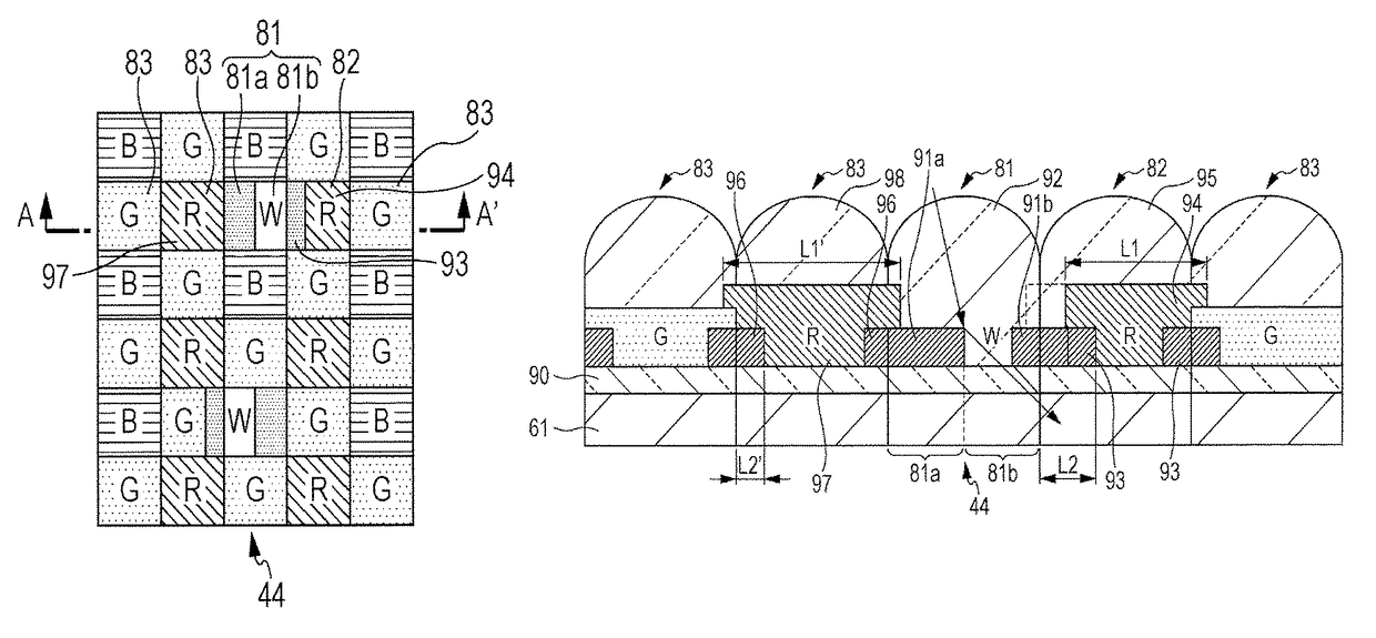
[0089](Configuration Example of an Illustrative Embodiment of Solid State Imaging Device)

[0090]FIG. 1 is a block diagram showing an illustrative configuration example of an embodiment of a solid state imaging device to which the present technology is applied.

[0091]A solid state imaging device 41 of FIG. 1 is configured to include, on a semiconductor substrate which is not shown, a timing control unit 42, a vertical scanning circuit 43, a pixel array unit 44, a constant current source circuit unit 45, a reference signal generation unit 46, a column AD conversion unit 47, a horizontal scanning circuit 48, a horizontal output line 49, and an output circuit 50.

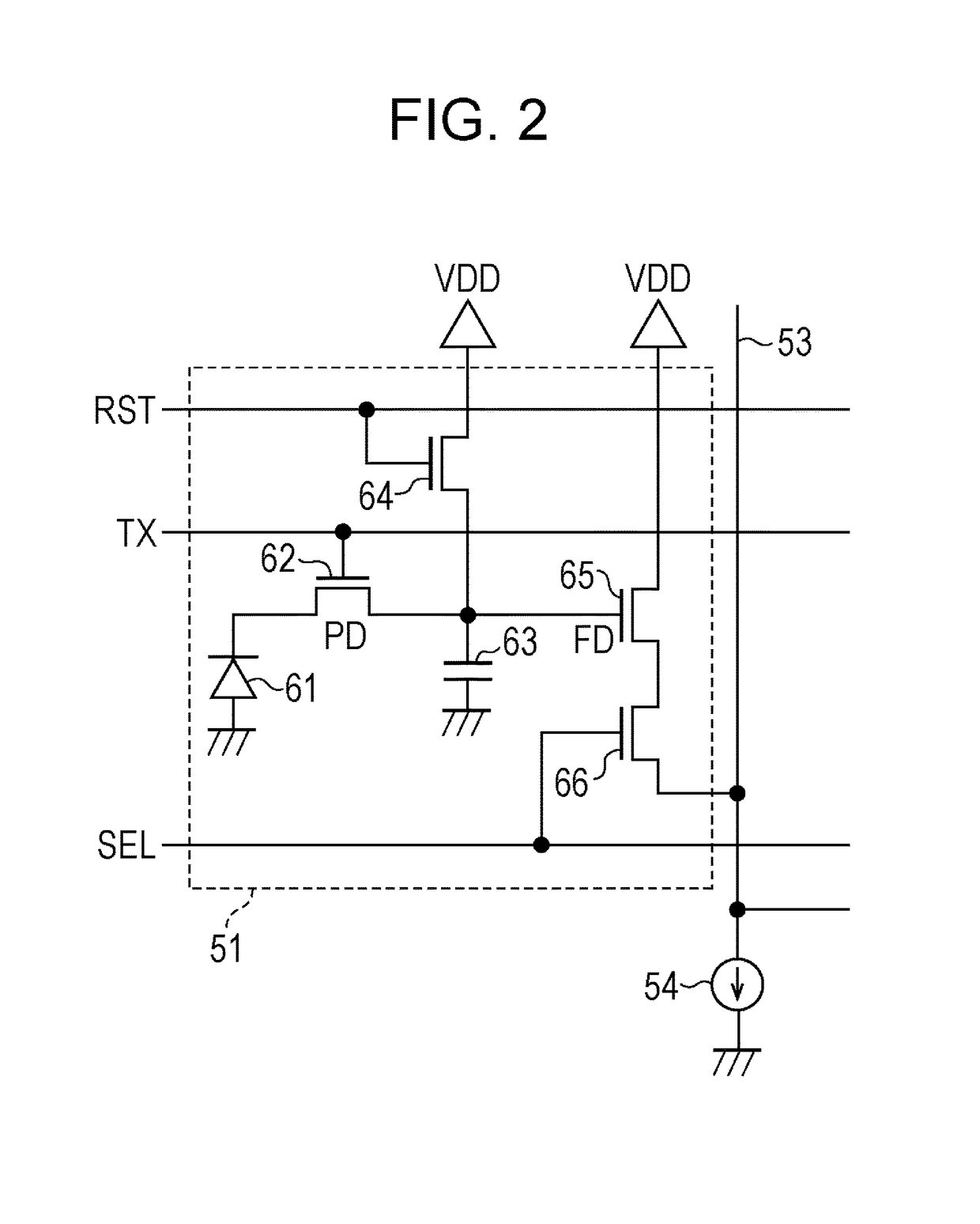
[0092]The timing control unit 42 supplies a clock signal or a timing signal, which is necessary for predetermined operations, to the vertical scanning circuit 43 and the horizontal scanning circuit 48 on the basis of a master clock of a predetermined frequency. For example, the timing control unit 42 s...


PUM


Abstract

A solid state imaging device that includes a phase difference detection pixel which is a pixel for phase difference detection; a first imaging pixel which is a pixel for imaging and is adjacent to the phase difference detection pixel; and a second imaging pixel which is a pixel for imaging other than the first imaging pixel. An area of a color filter of the first imaging pixel is smaller than an area of a color filter of the second imaging pixel.

Description

CROSS REFERENCE TO RELATED APPLICATIONS[0001]This application is a national stage application under 35 U.S.C. 371 and claims the benefit of PCT Application No. PCT / JP2014 / 006045 having an international filing date of Dec. 3, 2014, which designated the United States, which PCT application claimed the benefit of Japanese Patent Application No. 2013-257294 filed Dec. 12, 2013, and Japanese Patent Application No. 2014-109412 filed May 27, 2014, the disclosures of which are incorporated herein by reference in their entirety.TECHNICAL FIELD[0002]The present disclosure relates to a solid state imaging device, a manufacturing method of the same, and electronic equipment. In particular, the present disclosure relates to a solid state imaging device, a manufacturing method of the same, and electronic equipment which enable the suppression of color mixing and the suppression of sensitivity reduction in pixels for phase difference detection.CROSS REFERENCE TO RELATED APPLICATIONS[0003]This appl...

Claims


Application Information

Patent Timeline
Patent Type & Authority Patents(United States)
IPC IPC(8): H04N5/228H01L27/148H04N5/374H04N5/378H04N9/077H01L27/146
CPCH01L27/14645H01L27/14607H01L27/14612H01L27/14621H01L27/14623H01L27/14634H01L27/14685H01L27/14689H01L27/14818H04N5/374H04N5/378H04N9/077H04N25/76H04N9/01H04N25/75
Inventor TAYANAKA, HIROSHIINOUE, YUUJINAKATA, MASASHI
Owner SONY CORP
Why Eureka
Try Eureka