HSD liquid crystal display panel, display device and driving method thereof
a liquid crystal display panel and display device technology, applied in the direction of instruments, static indicating devices, etc., can solve the problems of increasing the difficulty of adjusting the display device, increasing the distortion of the display panel, etc., to achieve the effect of alleviating the wiring delay effect of data lines, reducing the equivalent impedance of the whole data line, and reducing the wiring delay
- Summary
- Abstract
- Description
- Claims
- Application Information
AI Technical Summary
Benefits of technology
Problems solved by technology
Method used
Image
Examples
example 1
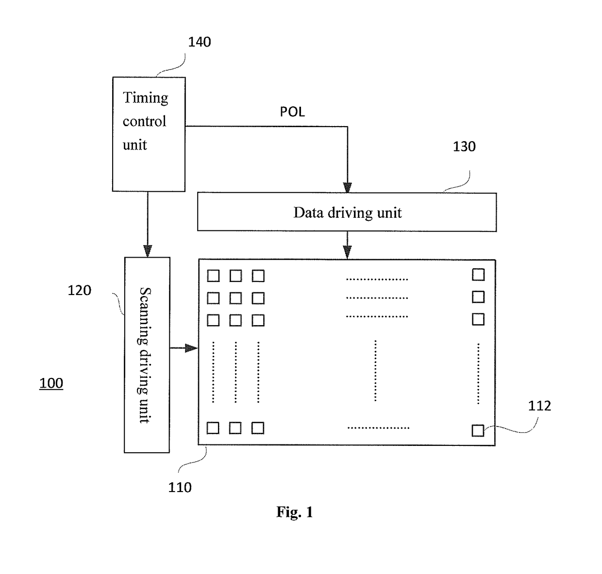
[0035]FIG. 1 is a structural schematic diagram of a HSD display device 100 according to the present Example. As shown in FIG. 1, the liquid crystal display device 100 comprises a display panel 110, a scanning driving unit 120, a data driving unit 130 and a timing control unit 140. The display panel 110 comprises a plurality of sub pixel units 112 arranged in a matrix form.
[0036]The scanning driving unit 120 and the data driving unit 130 are both electrically connected to the display panel 110. The timing control unit 140 is electrically connected to both of the scanning driving unit 120 and the data driving unit 130, in order to control the scanning driving unit 120 to scan the display panel 110 and control the data driving unit 130 to drive the display panel 110, so that the picture is displayed.
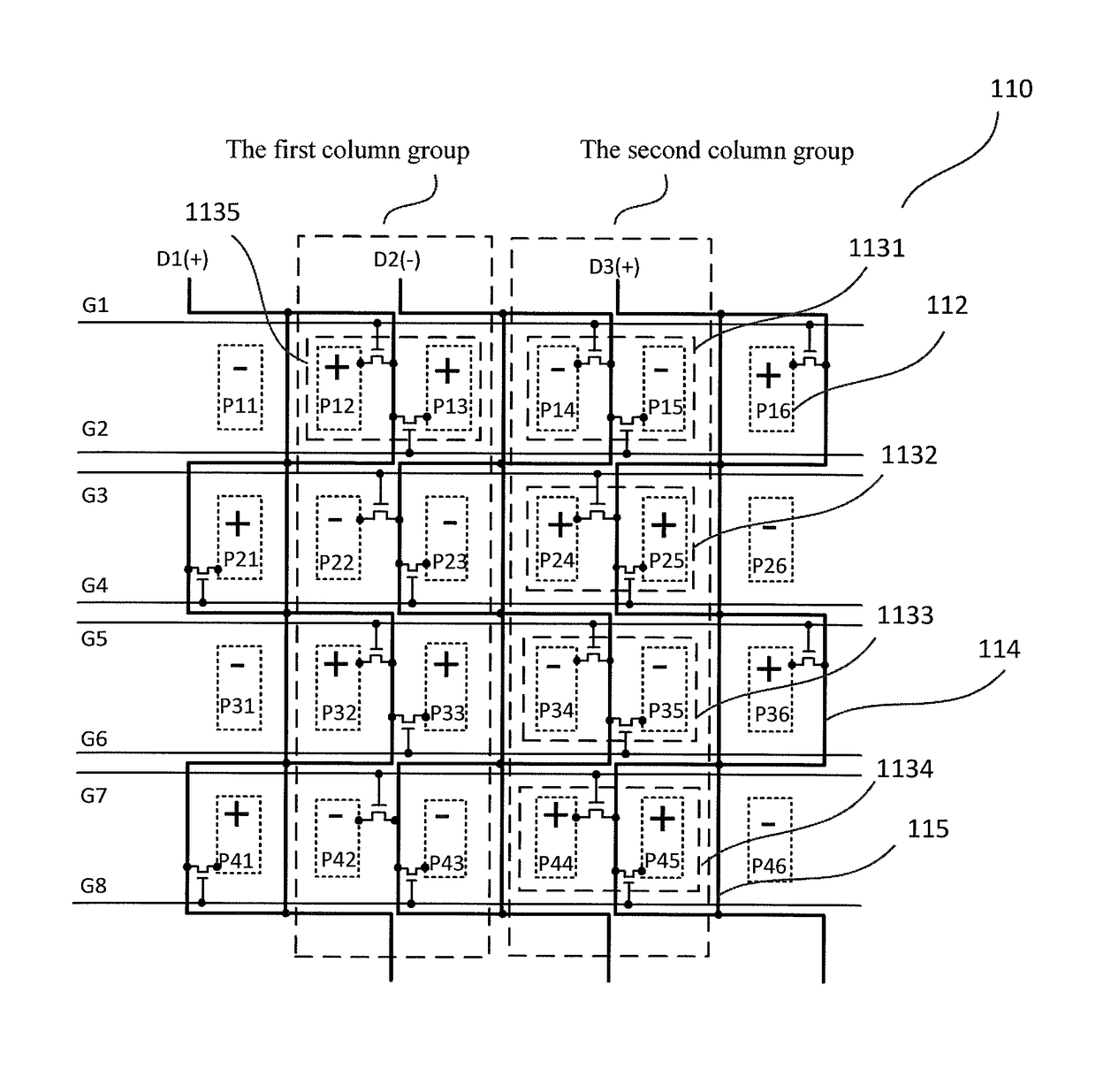
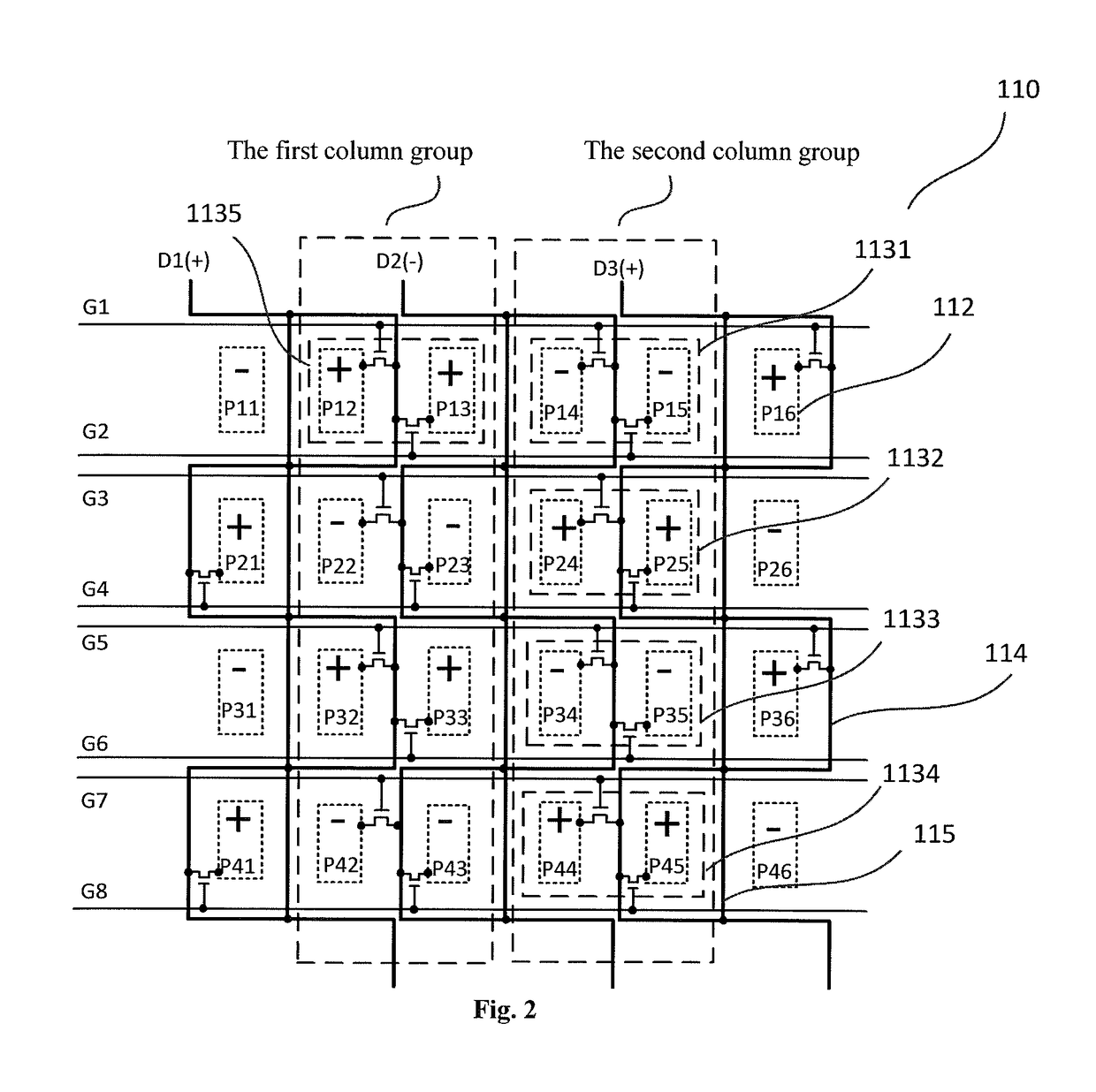
[0037]FIG. 2 is a structural schematic diagram of a display panel 110 according to the present example. In the present example, the display panel 110 comprises scanning lines G1 to G8 and d...
example 2
[0052]The present example provides a HSD display panel and a HSD display device. FIG. 7 is a structural schematic diagram of a HSD display panel according to the present example. The arrangement mode of sub pixel units and the number of winding parts in each data line of the display panel 700 are different from those of Example 1. In FIG. 7, the scanning lines are connected to sub pixel units in the same way as Example 1, and thus the scanning lines are not shown in FIG. 7 for simplicity.
[0053]In the present example, each sub pixel unit group comprises four sub pixel units arranged in a matrix form, and each column group comprises a plurality of sub pixel unit groups that are connected to adjacent data lines and arranged vertically. For example, the sub pixel unit group 711 comprises sub pixel units P14, P15, P24, and P25, which are arranged on both sides of the data line D2 respectively. The second column group comprises sub pixel unit groups 711 and 713 connected to the data line ...
PUM
 Abstract
Description
Claims
Application Information


