Organic light emitting display and driving method thereof

a technology of light-emitting display and organic light-emitting display, which is applied in the direction of instruments, static indicating devices, etc., can solve the problems of reducing the brightness of pixels gradually, reducing the life of organic light-emitting display, and reducing so as to ensure the operation margin of driving circuit.

Active Publication Date: 2008-06-26
SAMSUNG DISPLAY CO LTD
View PDF10 Cites 151 Cited by
  • Summary
  • Abstract
  • Description
  • Claims
  • Application Information

AI Technical Summary

Benefits of technology

[0010]The present invention has been contrived to solve the conventional problems as described above, and an aspect of the present invention is to ensure an operation margin of a driving circuit when driving a la

Problems solved by technology

If using the progressive scanning method, it has an advantage in that it provides an excellent image quality in a static screen; however, it also has drawbacks in that it is difficult to ensure an operation margin of a driving circuit when driving a large-size panel, since its scanning rate is no more than half that of the interlaced scanning method.
Moreover, the progressive scanning method has drawbacks in that it may cause a voltage drop (I

Method used


Image

  • Organic light emitting display and driving method thereof
  • Organic light emitting display and driving method thereof
  • Organic light emitting display and driving method thereof

Examples


Embodiment Construction

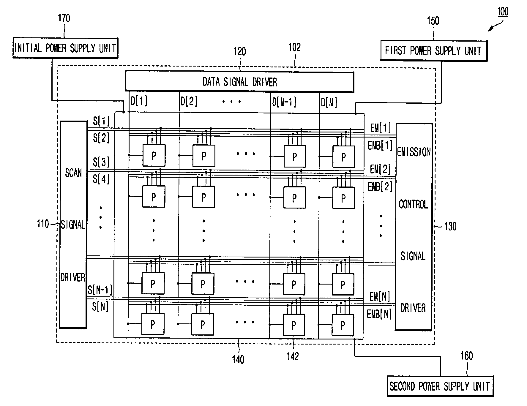
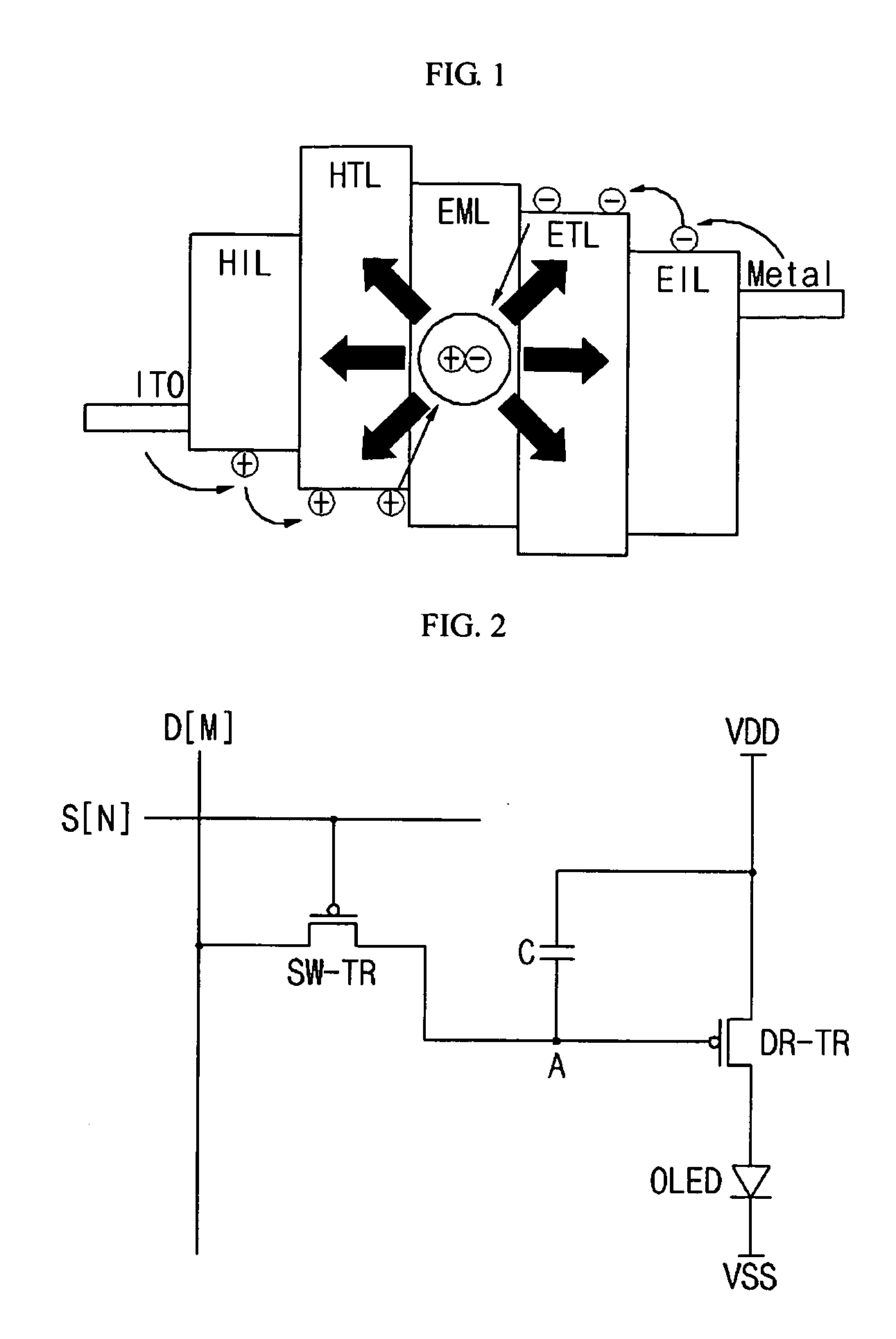
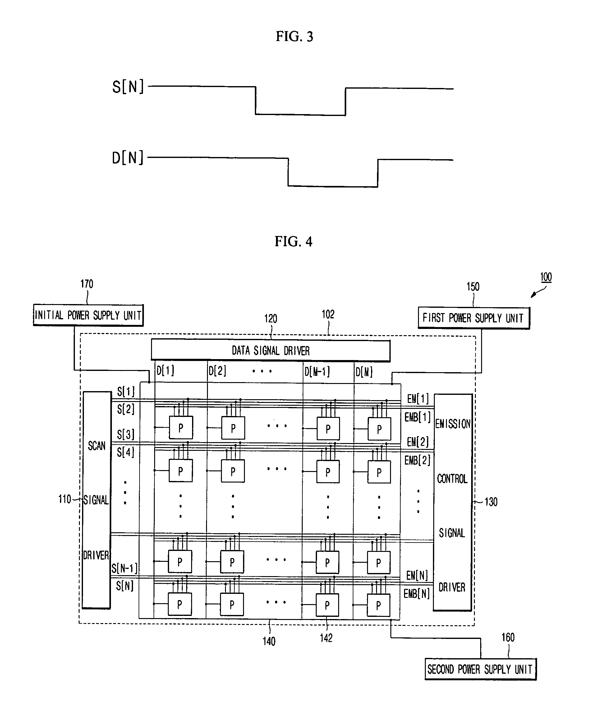
[0037]The present invention now will be described more fully hereinafter with reference to the accompanying drawings, in which exemplary embodiments of the invention are shown. This invention may, however, be embodied in many different forms and should not be construed as limited to the embodiments set forth herein; rather, these embodiments are provided so that this disclosure will be thorough and complete, and will fully convey the scope of the invention to those having skill in the art.

[0038]For the purpose of explaining the present invention explicitly, the portions unrelated to the present invention are omitted in the drawings. Throughout the specification of the present invention, the elements having the same configuration and operation are denoted by the same reference numerals. Supposed that a certain portion is coupled to another portion, it includes the case where it is connected to the same via a different element as well as the case where it is directly connected to the ...


PUM


Abstract

An organic light emitting display including a scan signal line forwarding a scan signal, a data line sending a data signal and a pixel coupled to the scan signal line and the data line, the organic light emitting diode display, wherein the pixel includes a first switching transistor transmitting a data signal from the data line in response to the scan signal of the scan signal line, a driving transistor, coupled to the first switching transistor, controlling driving current from a first power source line, a storage capacitor coupled between the driving transistor and the first power source line, an organic light emitting diode, coupled between the driving transistor and a second power source line, displaying an image with the driving current controlled by the driving transistor, an initial switching transistor, coupled between the storage capacitor and an initial power source line, initializing the storage capacitor, and a switching transistor for applying a reverse bias, coupled between the second power source line and the initial power source line, applying a reverse bias voltage to the organic light emitting diode.

Description

CROSS-REFERENCE TO RELATED APPLICATIONS[0001]This application claims the benefit of Korean Patent Application No. 10-2006-0131962 filed on Dec. 21, 2006, in the Korean Intellectual Property Office, the disclosure of which is incorporated herein by reference.BACKGROUND[0002]1. Field of the Invention[0003]The present invention relates to an organic light emitting display and a driving method thereof and, more particularly, to an organic light emitting display and a driving method thereof that ensure an operation margin of a driving circuit when driving a large-size panel by applying an interlaced scanning method, prevent a voltage drop (IR-drop) of a first power source line VDD and, simultaneously, minimize degradation of the organic light emitting diode OLED in a pixel circuit of the organic light emitting display by dividing a data write period from a light emission period in driving the panel.[0004]2. Discussion of Related Art[0005]Recently, the organic light emitting display has a...

Claims


Application Information

Patent Timeline
IPC IPC(8): G09G3/30
CPCG09G3/3233G09G2300/0819G09G2300/0842G09G2320/043G09G2310/0224G09G2310/0256G09G2300/0861G09G3/3258H10K59/10
Inventor CHUNG, BOYONG
Owner SAMSUNG DISPLAY CO LTD
Why Eureka
Try Eureka