Semiconductor wafer inspection apparatus and semiconductor wafer inspection method

a technology of semiconductor wafers and inspection apparatus, which is applied in the direction of conveyor parts, instruments, transportation and packaging, etc., can solve the problems of difference in thermal expansion between the bottom surface and the semiconductor wafer, and achieve the effect of suppressing the warpage of the semiconductor wafer

Active Publication Date: 2018-01-16
TOKYO SEIMITSU
View PDF10 Cites 1 Cited by
  • Summary
  • Abstract
  • Description
  • Claims
  • Application Information

AI Technical Summary

Benefits of technology

[0032]By the one aspect of the present invention, it is possible to avoid disadvantageous effects due to a temperature difference between the mounting surface of the table and the semiconductor wafer, and convey the semiconductor wafer in the shortest time.
[0033]A semiconductor wafer inspection apparatus and a semiconductor wafer inspection method of the present invention can suppress warpage of a semiconductor wafer due to a difference in temperature between the mounting surface of a table and the semiconductor wafer.

Problems solved by technology

However, a significantly large difference between the temperatures of the mounting surface of the table and the semiconductor wafer causes a problem of warpage in the semiconductor wafer right after the placement of the semiconductor wafer on the mounting surface of the table.
This problem results from a difference in thermal expansion between the bottom surface of the semiconductor wafer in contact with the mounting surface of the table and the top surface of the semiconductor wafer exposed to air, that is, a temperature gradient due to the thickness of the semiconductor wafer.

Method used


Image

  • Semiconductor wafer inspection apparatus and semiconductor wafer inspection method
  • Semiconductor wafer inspection apparatus and semiconductor wafer inspection method
  • Semiconductor wafer inspection apparatus and semiconductor wafer inspection method

Examples


Embodiment Construction

[0041]A semiconductor wafer inspection apparatus and a semiconductor wafer inspection method according to a preferred embodiment of the present invention will now be described with reference to the attached drawings.

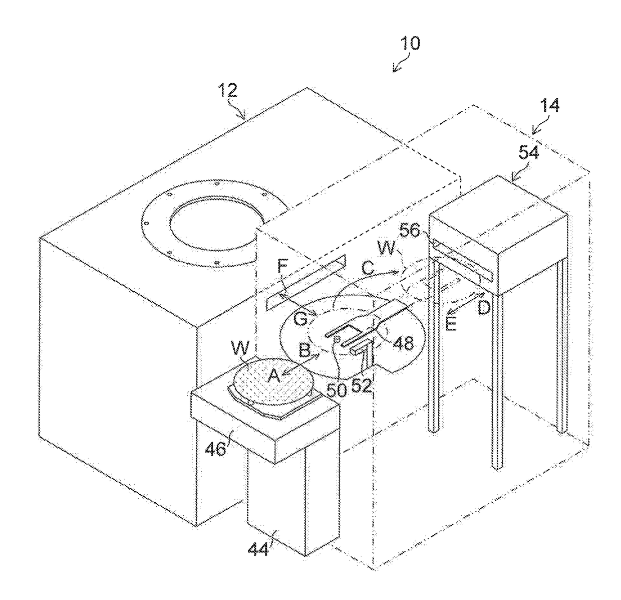
[0042]FIG. 1 is a general perspective view illustrating the structure of a prober (semiconductor wafer inspection apparatus) 10 according to an embodiment to which the semiconductor wafer inspection apparatus and the semiconductor wafer inspection method of the present invention are applied.

[0043][Structure of Prober 10]

[0044]The prober 10 includes a prober body 12 and a loader unit 14 adjacent to the prober body 12. It should be noted that FIG. 1 illustrates the loader unit 14 in perspective in order to schematically show the internal structure of the loader unit 14.

[0045]12>

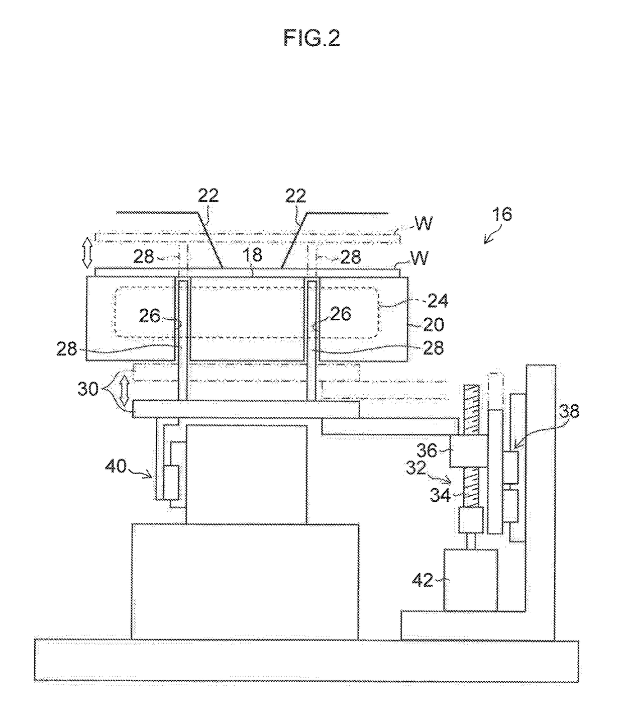
[0046]FIG. 2 is a side view of an inspecting unit 16 disposed inside the prober body 12 (see FIG. 1).

[0047]The inspecting unit 16 includes a table 20 having a mounting surface 18 on which a semicond...


PUM


Abstract

The present invention provides a semiconductor wafer inspection apparatus and a semiconductor wafer inspection method that can suppress warpage in a semiconductor wafer due to a temperature difference between the mounting surface of a table and the semiconductor wafer. In a prober of the present invention, a semiconductor wafer is heated to have a second temperature which is equal to or lower than a first temperature in a preheating step using an oven, and then the semiconductor wafer is placed on a mounting surface of a table which is heated to the first temperature. Thus, because a temperature difference between the mounting surface of the table and the semiconductor wafer is reduced in the prober, it is possible to suppress warpage in the semiconductor wafer that occurs right after the semiconductor wafer is placed on the mounting surface.

Description

CROSS-REFERENCE TO RELATED APPLICATIONS[0001]This application is a Continuation of PCT International Application No. PCT / JP2015 / 070855 filed on Jul. 22, 2015, which claims priority under 35 U.S.C. §119 to Japanese Patent Application No. 2014-253947 filed on Dec. 16, 2014. Each of the above applications is hereby expressly incorporated by reference, in their entirety, into the present application.BACKGROUND OF THE INVENTION[0002]1. Field of the Invention[0003]The present invention relates to a semiconductor wafer inspection apparatus and a semiconductor wafer inspection method, and particularly to a semiconductor wafer inspection apparatus and a semiconductor wafer inspection method for inspecting electronic devices on a semiconductor wafer for electric characteristics.[0004]2. Description of the Related Art[0005]In a semiconductor manufacturing process, a plurality of chips with electronic devices are produced through various treatments to a thin plate-like semiconductor wafer. The ...

Claims


Application Information

Patent Timeline
Patent Type & Authority Patents(United States)
IPC IPC(8): G01R31/28H01L21/687G01R31/00H01L21/683G01R1/067H01L21/677H01L21/67
CPCG01R31/2875G01R1/06705G01R31/00H01L21/677H01L21/68742H01L21/67109H01L21/67115H01L21/683H01L21/67103G01R31/2862
Inventor ISHIMOTO, TAKASHISHIGESAWA, YUJIYAMAGUCHI, AKIRAMOTOYAMA, TAKASHITAKAHASHI, TAKENORI
Owner TOKYO SEIMITSU
Why Eureka
Try Eureka