N+ poly on high-k dielectric for semiconductor devices

a technology of dielectric and polysilicon, which is applied in the direction of semiconductor devices, basic electric elements, electrical equipment, etc., can solve the problems of degrading the performance of a pmos device, achieve the effects of reducing the size of the device, reducing the undesirable effect, and facilitating semiconductor fabrication

Active Publication Date: 2006-10-05
TEXAS INSTR INC
View PDF9 Cites 145 Cited by
  • Summary
  • Abstract
  • Description
  • Claims
  • Application Information

AI Technical Summary

Benefits of technology

[0008] The present invention provides systems and methods that facilitate semiconductor fabrication by integrating high-k dielectric layers and polysilicon gate layers into the process flow. Use of polysilicon gates and high-k dielectric layers can permit decreased device size and -improved device performance, but do present some problems such as threshold voltage shift. Undesirable effects resulting from the inclusion of the high-k dielectric layers with the polysilicon gate layers, particularly with respect to PMOS devices, are mitigated by the present invention. An n-type doped polysilicon gate layer and a counter doping, threshold voltage implant are employed in order to mitigate the undesirable affects. The n-type doped polysilicon gate layer mitigates or eliminates poly depletion, which otherwise degrades performance of a PMOS device. The n-type doped polysilicon gate layer and the high-k dielectric layer result in a known threshold voltage shift, instead of a variable, uncontrolled shift. The counter doping, because the shift is known and predictable, can be employed to account for that shift.

Problems solved by technology

Use of polysilicon gates and high-k dielectric layers can permit decreased device size and -improved device performance, but do present some problems such as threshold voltage shift.
The n-type doped polysilicon gate layer mitigates or eliminates poly depletion, which otherwise degrades performance of a PMOS device.

Method used


Image

  • N+ poly on high-k dielectric for semiconductor devices
  • N+ poly on high-k dielectric for semiconductor devices
  • N+ poly on high-k dielectric for semiconductor devices

Examples


Embodiment Construction

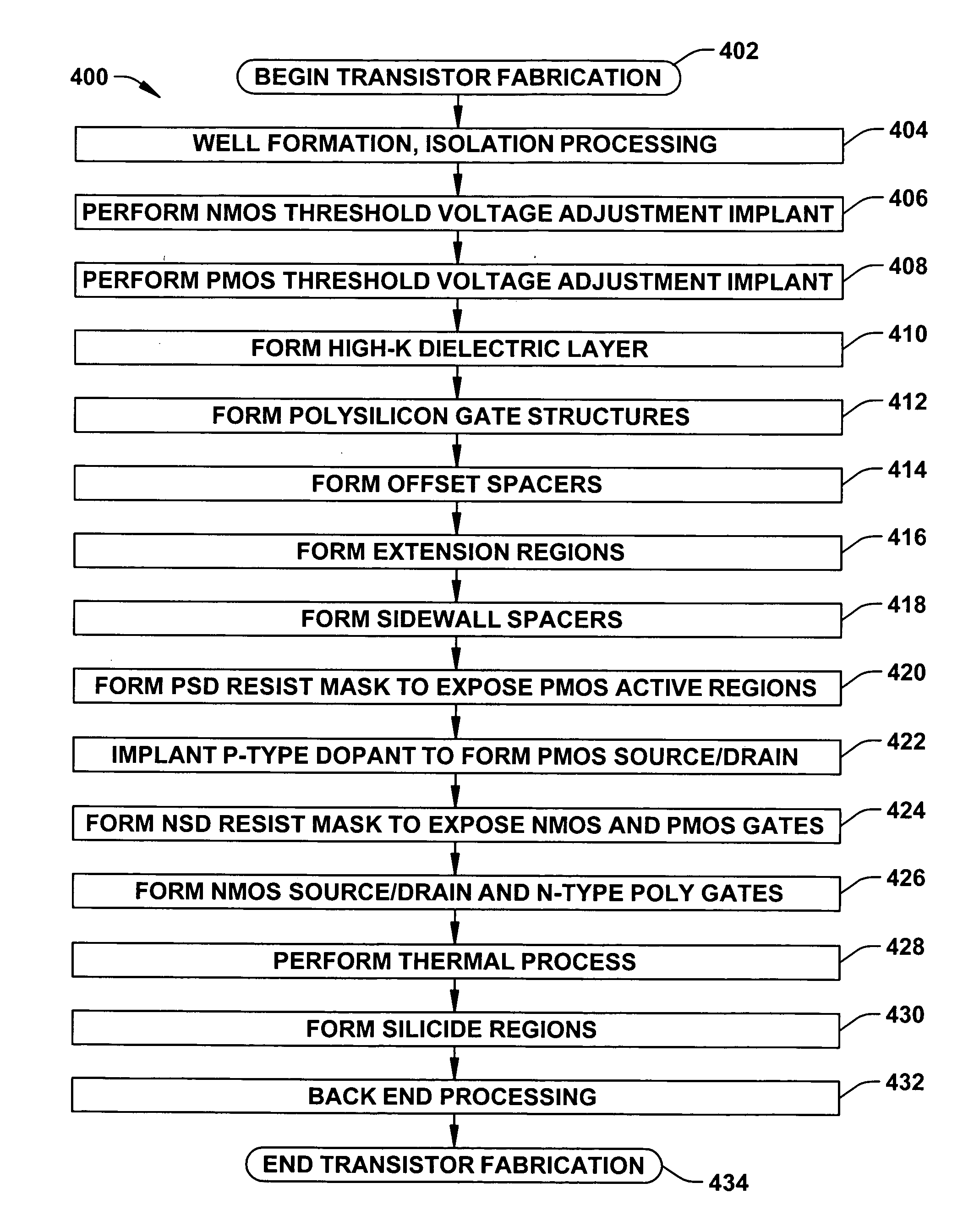
[0016] One or more implementations of the present invention will now be described with reference to the attached drawings, wherein like reference numerals are used to refer to like elements throughout, and wherein the illustrated structures are not necessarily drawn to scale. The invention provides transistor structures and methods in which transistor mobility is improved while reducing masks employed in fabrication thereof.

[0017] The present invention facilitates semiconductor fabrication by providing methods of fabrication that integrate high-k dielectric layers and polysilicon gate layers into the process flow. Use of polysilicon gates and high-k dielectric layers can permit decreased device size and improved device performance, but do present some problems such as threshold voltage shift. Undesirable effects resulting from the inclusion of the high-k dielectric layers with the polysilicon gate layers, particularly with respect to PMOS devices, are mitigated by the present inven...


PUM


Abstract

The present invention facilitates semiconductor fabrication by providing methods of fabrication that employ high-k dielectric layers. An n-type well region (304) is formed within a semiconductor body (302). A threshold voltage adjustment implant is performed by implanting a p-type dopant into the n-type well region to form a counter doped region (307). A high-k dielectric layer (308) is formed over the device (300). A polysilicon layer (310) is formed on the high-k dielectric layer and doped n-type. The high-k dielectric layer (308) and the polysilicon layer (310) are patterned to form polysilicon gate structures. P-type source / drain regions (306) are formed within the n-type well region (304).

Description

FIELD OF INVENTION [0001] The present invention relates generally to semiconductor devices and more particularly to transistor devices having high-k dielectric layers and polysilicon gate layers and associated methods of manufacture. BACKGROUND OF THE INVENTION [0002] Field effect transistors (FETs) are widely used in the electronics industry for switching, amplification, filtering, and other tasks related to both analog and digital electrical signals. Most common among these are metal-oxide-semiconductor field-effect transistors (MOSFET or MOS), in which a gate is energized to create an electric field in an underlying channel region of a semiconductor body, by which electrons are allowed to travel through the channel between a source region and a drain region of the semiconductor body. Complementary MOS (CMOS) devices have become widely used in the semiconductor industry, wherein both n-channel and p-channel (NMOS and PMOS) transistors are used to fabricate logic and other circuitr...

Claims


Application Information

Patent Timeline
Patent Type & Authority Applications(United States)
IPC IPC(8): H01L21/336
CPCH01L21/26506H01L21/823807H01L29/7838H01L29/517H01L21/823857H01L21/26513
Inventor VENUGOPAL, RAMESHWASSHUBER, CHRISTOPHSCOTT, DAVID BARRY
Owner TEXAS INSTR INC
Why Eureka
Try Eureka