Method for plating using nested plating buses and semiconductor device having the same

a plating bus and bus technology, applied in the direction of conductive pattern reinforcement, electrical apparatus construction details, association of printed circuit non-printed electric components, etc., can solve the problems of restriction in routing electrical connections from the vias, single layer substrates, and the most expensive individual cost components

Inactive Publication Date: 2000-07-11
FREESCALE SEMICON INC
View PDF15 Cites 75 Cited by
  • Summary
  • Abstract
  • Description
  • Claims
  • Application Information

AI Technical Summary

Problems solved by technology

The most expensive individual cost component is the substrate.
One of the limitations of single layer substrates is the restriction in routing electrical connections from the vias to an external plating bus formed at the periphery of the package.
Depending on the capabilities of the substrate manufacturer and on the I / O count of the package, the external plating connections also often directly limit the number of discrete I / O connections possible for single layer substrate packages.
In other words, the need to connect all traces to an external, peripheral plating bus often restricts the routing density for a given size substrate.
Increasing the solder pad and via pitches undesirably increases the size of the substrate and size of the final package, whereas decreasing solder pad and via diameters would undesirably increase the cost to manufacture the substrate and reduce the solder joint strength due to the smaller solder pads.
However, electroless plating is inherently thinner and more porous than electrolytic plating which makes it marginal at preventing oxidation of the underlying copper.
This in turn makes it more difficult to achieve good, reliable bonding onto the plated surfaces.
Consequently, the use of electroless gold plating is limited to special cases where the time and temperature exposures are short and low enough that the resulting oxidation does not impede the creation of reliable bonds.

Method used


Image

  • Method for plating using nested plating buses and semiconductor device having the same
  • Method for plating using nested plating buses and semiconductor device having the same
  • Method for plating using nested plating buses and semiconductor device having the same

Examples


Embodiment Construction

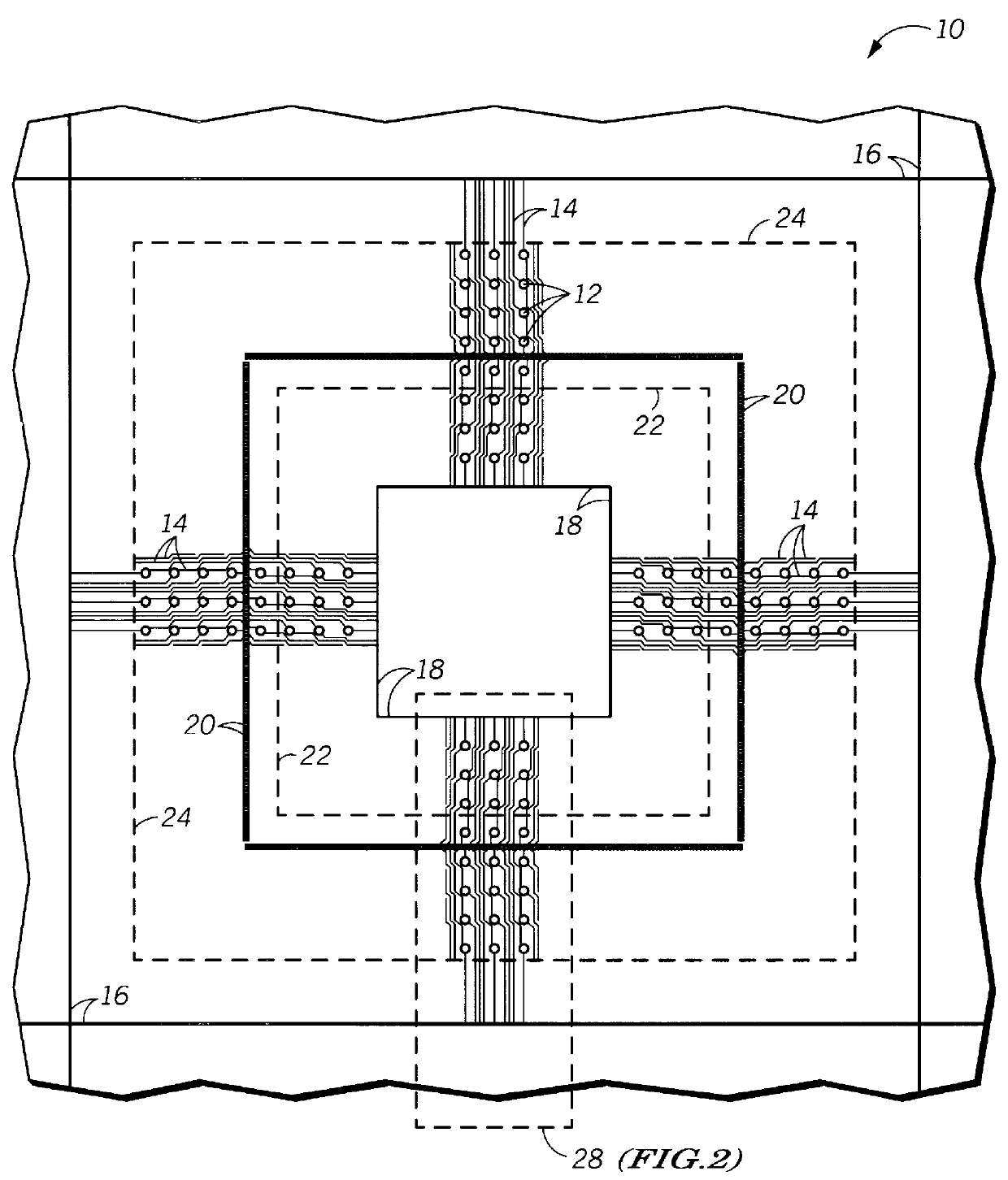
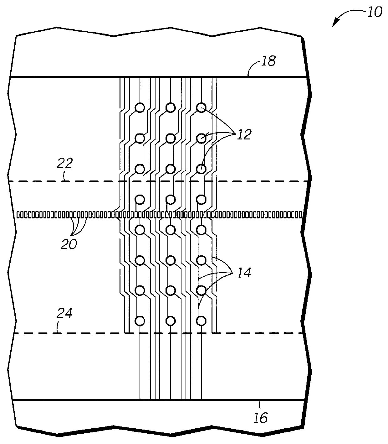
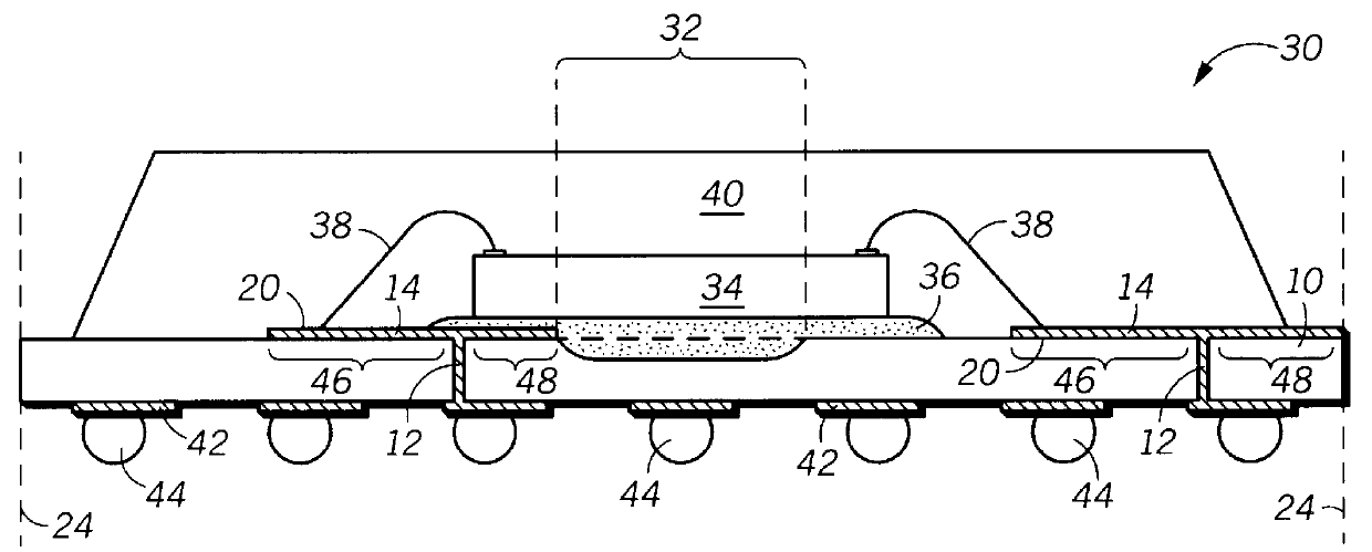
The present invention increases the maximum possible I / O count for a given substrate size by allowing a nested plating bus to complement the existing external plating bus. In addition, the use of the nested plating bus reduces or eliminates the need for bottom side electrical routing which should improve package reliability and electrical performance by increasing the distance between discrete conductive traces, vias and solder pads on the bottom side of the substrate.

These and other features, and advantages, of the present invention will be more clearly understood from the following detailed description taken in conjunction with the accompanying drawings. It is important to point out that the illustrations may not necessarily be drawn to scale, and that there may be other embodiments of the present invention which are not specifically illustrated. Also, like reference numerals may be used throughout the various views, indicating identical, corresponding, or similar elements.

FIG. 1 ...


PUM

PropertyMeasurementUnit
widthaaaaaaaaaa
diameteraaaaaaaaaa
diameteraaaaaaaaaa

Abstract

Routing density of a wiring substrate (10) is increased by providing a nested plating bus (18) as a supplement to an external plating bus (16). A first group of conductive traces (14) is connected to the nested plating bus, while another group of traces is connected to the external plating bus. After the conductive elements are plated, the nested plating bus is removed by etching, milling, or stamping techniques. Use of a nested plating bus increases I / O count for a given substrate area and / or reduces the need to have routing on more than one layer of the substrate.

Description

FIELD OF THE INVENTIONThe present invention relates to plating and plated devices in general, and more specifically to plating using nested plating buses and semiconductor devices having such nested plating buses.BACKGROUND OF THE INVENTIONDue to the constant push for smaller and smaller products, it has become common for integrated circuits (ICs) once contained on two or more individual semiconductor die or chips to be combined into a single, larger IC device. For example, traditional microprocessor circuits are being combined on a single chip with digital signal process circuits. These combined ICs have the advantage of better reliability due to fewer total external connections, but have higher input / output (I / O) counts than many of the individual ICs. Often, these combined devices have I / Os in the 200+ range. Additionally, new ICs are being designed "from the ground up" with many advanced features which also result in 200+ I / Os. Thus, high I / O counts are becoming more and more co...

Claims


Application Information

Patent Timeline
Patent Type & Authority Patents(United States)
IPC IPC(8): H05K7/02H01L21/58H01L23/31H01L23/498H05K3/00H05K3/24
CPCH01L23/3128H01L23/49838H01L24/32H01L24/83H01L23/49816Y10T29/49144H01L2224/32057H01L2224/32225H01L2224/48091H01L2224/48227H01L2224/73265H01L2224/8319H01L2224/83385H01L2224/8385H01L2924/01029H01L2924/01078H01L2924/01079H01L2924/01082H01L2924/07802H01L2924/14H01L2924/15311H05K3/0097H05K3/241H01L2924/014H01L2924/01076H01L2924/01033H01L2924/01006H01L24/48H01L2924/00014H01L2924/00012H01L2924/15787H01L2224/451H01L24/45H01L24/73H01L2924/181H01L2924/15183H01L2924/00H01L2224/45099H05K7/02
Inventor NOMI, VICTOR K.PASTORE, JOHN R.REEVES, TWILA J.
Owner FREESCALE SEMICON INC
Why Eureka
Try Eureka