Method of manufacturing display device
一种显示器件、激励器的技术,应用在电固体器件、静态指示器、半导体器件等方向
- Summary
- Abstract
- Description
- Claims
- Application Information
AI Technical Summary
Problems solved by technology
Method used
Image

Examples
Embodiment 1
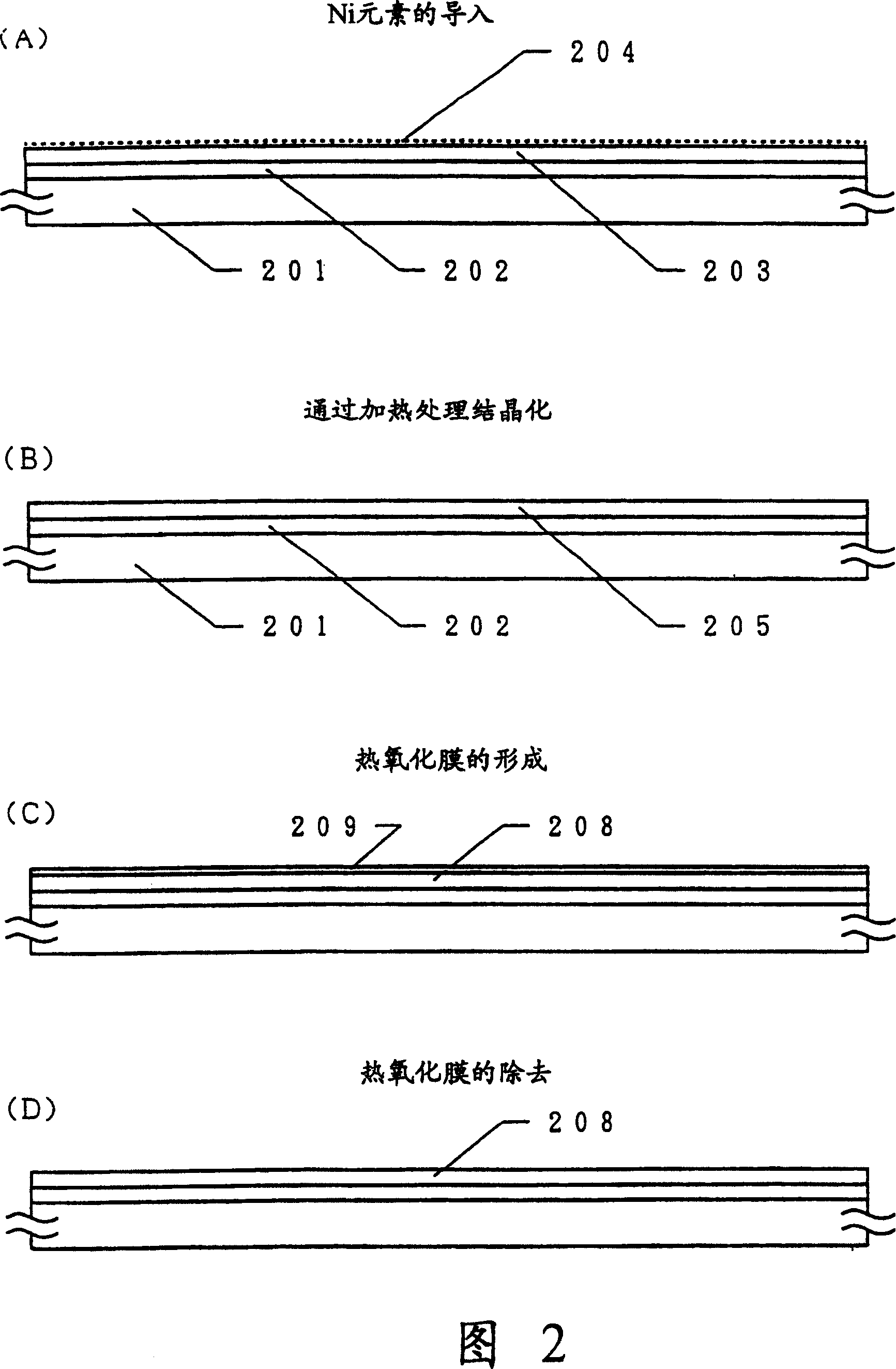
[0071](Example 1) In this example, a method of non-selectively introducing a metal element that promotes silicon crystallization to the entire surface of an amorphous silicon film will be described, and a process for producing a TFT using the silicon crystal film will be described.
[0072] Fig. 2 shows the manufacturing process of this embodiment. First, a silicon oxide film serving as the base film 202 is formed on a quartz substrate 201 to a thickness of 3000 Ȧ. The base film 202 is unnecessary if the surface of the quartz substrate is smooth and sufficiently cleaned.
[0073] In addition, as the substrate, it is preferable to use a quartz substrate, but if there is a substrate that can withstand the heat treatment temperature, it is not limited to quartz. For example, a semiconductor substrate on which an oxide film is formed can also be used. Next, an amorphous film 203, which is a starting film of a silicon crystal film, is formed to a thickness of 500 Ȧ by a reduced-p...
Embodiment 2
[0096] (Example 2) This example relates to a method of performing crystal growth in a parallel direction on a substrate called lateral growth by selectively introducing a catalytic element that contributes to silicon crystallization into an amorphous silicon film. Fig. 4 shows the manufacturing process of this embodiment.
[0097] First, a silicon oxide film with a thickness of 3000 Ȧ was formed as the base film 402 on the quartz substrate 401 . Next, an amorphous silicon film 403 having a thickness of 500 Ȧ was formed as a silicon crystal film starting film by thermal decompression CVD.
[0098] Next, a silicon oxide film having a thickness of 1500 Ȧ is formed and etched to form a mask indicated by 404 . The mask forms openings in the areas indicated at 405 . In the region where the opening 405 is formed, the amorphous silicon film 403 is exposed.
[0099] The opening 405 is an elongated rectangle having a longitudinal axis in the depth direction and the front direction of...
Embodiment 3
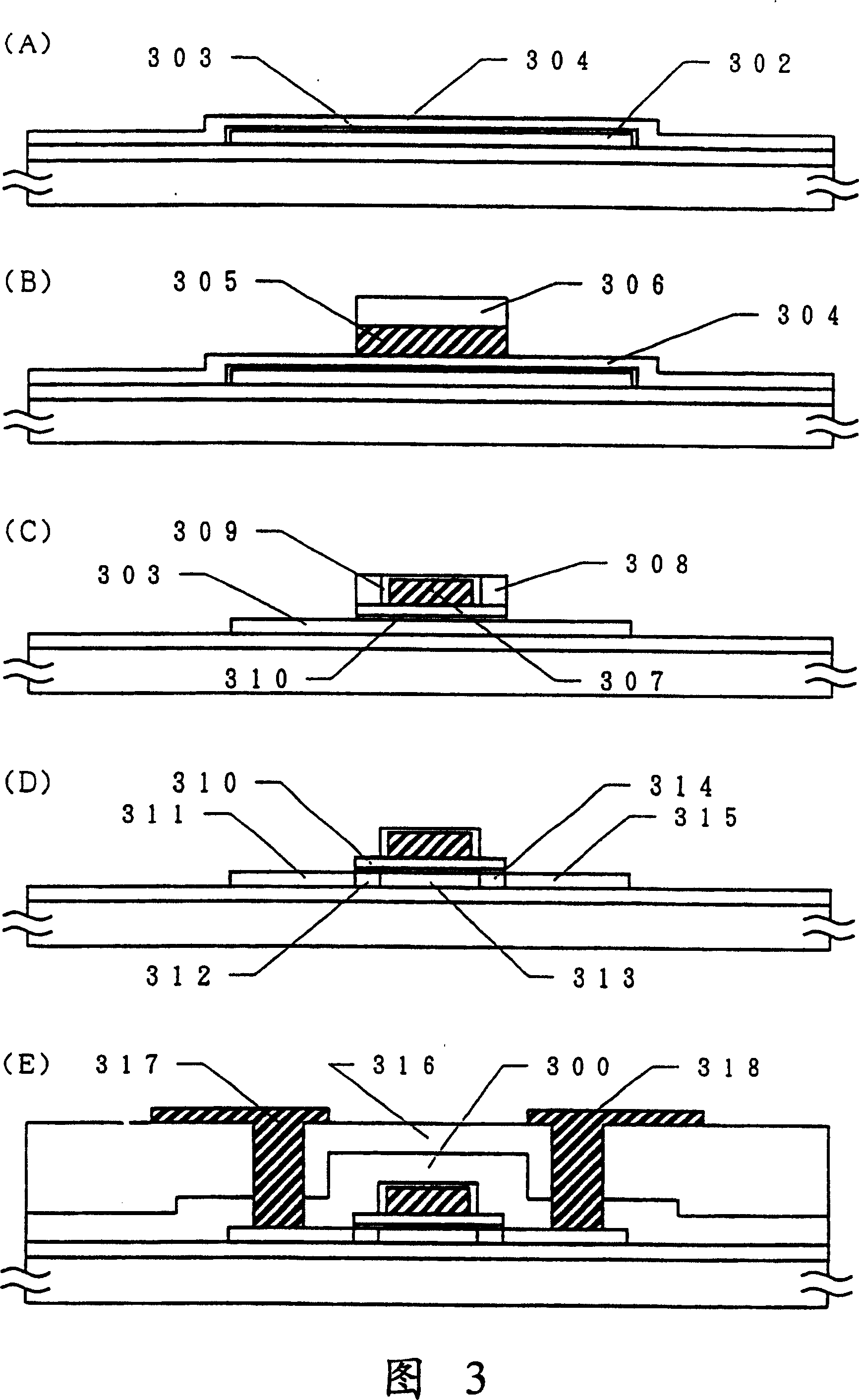
[0125] (Embodiment 3) This embodiment relates to a method of forming a gate insulating film in the structure shown in Embodiment 2. Fig. 6 shows the manufacturing process of this embodiment. First, a silicon crystal film 408 with a lateral growth region is obtained according to the process shown in FIG. 4(A) and FIG. 4(B). In addition, here, the amorphous silicon film of the starting film is 500 Ȧ.
[0126] After the silicon crystal film 408 was obtained, a thermal oxide film 409 was formed to a thickness of 200 Ȧ by performing heat treatment at 950° C. in an oxygen atmosphere containing 3% HCl. (Figure 6(A))
[0127] Next, the thermal oxide film 409 is removed. Furthermore, the silicon film is etched to form a pattern 410 as the active layer of the subsequent thin film transistor. (Figure 6(B))
[0128] Subsequently, an insulating film 504 is formed by a plasma CVD method. As the CVD insulating film 504, a silicon oxide film or a silicon nitride film 504 is formed to a ...
PUM
 Abstract
Description
Claims
Application Information
 - R&D
- Intellectual Property
- Life Sciences
- Materials
- Tech Scout
- Unparalleled Data Quality
- Higher Quality Content
- 60% Fewer Hallucinations
Browse by: Latest US Patents, China's latest patents, Technical Efficacy Thesaurus, Application Domain, Technology Topic, Popular Technical Reports.
© 2025 PatSnap. All rights reserved.Legal|Privacy policy|Modern Slavery Act Transparency Statement|Sitemap|About US| Contact US: help@patsnap.com