Low-voltage conrol method and device

A technology of working voltage and control circuit, which is applied in the direction of static memory, instrument, transistor, etc., and can solve the problems of DRAM internal circuit false triggering and circuit failure

Inactive Publication Date: 2007-11-21
SAMSUNG ELECTRONICS CO LTD
View PDF5 Cites 0 Cited by
  • Summary
  • Abstract
  • Description
  • Claims
  • Application Information

AI Technical Summary

Problems solved by technology

Large electrical surges cause severe strain on the battery, generating heat and potentially disabling circuits
In addition, some nodes in the circuit that are turned off may drift to unspecified voltages, and if the circuit is not properly turned on, false triggering of the internal circuits of the DRAM may also occur

Method used


Image

  • Low-voltage conrol method and device
  • Low-voltage conrol method and device
  • Low-voltage conrol method and device

Examples


Embodiment Construction

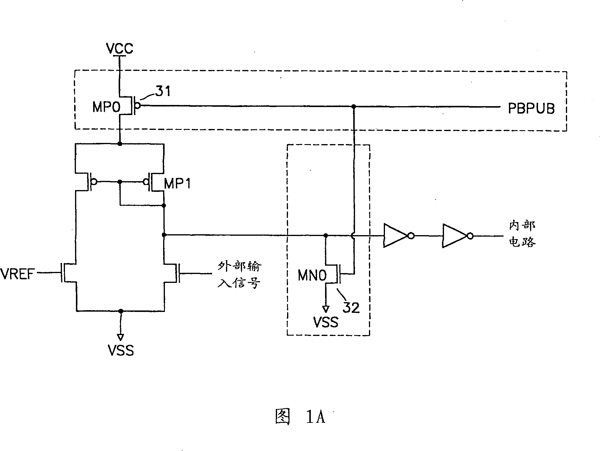
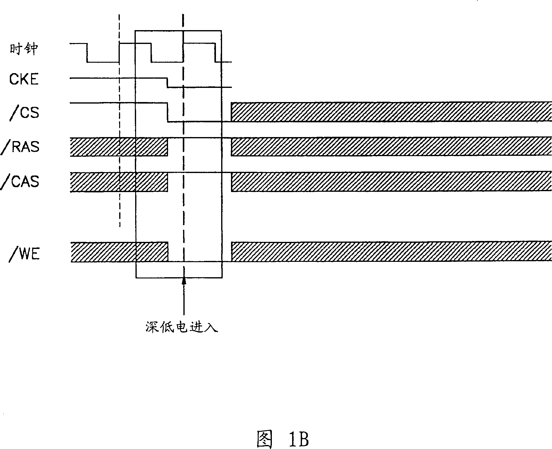
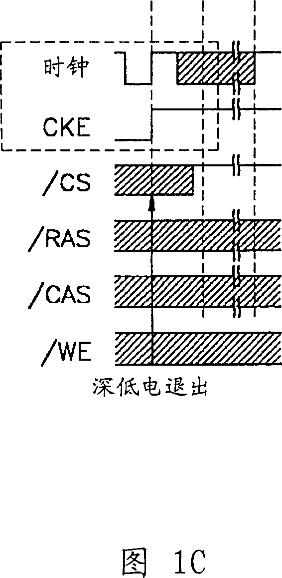
[0042] According to a preferred embodiment of the present invention, there are provided apparatus and methods for operating internal circuits of a DRAM upon entering, exiting, and in a power saving mode of operation. According to several aspects of the present invention, leakage current during power saving mode is reduced or eliminated, the amount of surge during circuit turn-on when exiting power saving mode is reduced, and false triggering of internal circuits is eliminated. Preferred embodiments of the present invention are used to reduce surges when the input buffer and internal power voltage generator are switched on when a semiconductor device enters or exits DPD mode. According to a preferred embodiment of the present invention, for example, by varying the settling time of switching on of the internal power voltage generators, varying the driving capabilities of different internal power voltage generators or buffers, delaying the switching on of different voltage generat...


PUM


Abstract

A semiconductor device for controlling entry to and exit from a power down mode (DPD) of a semiconductor memory, comprising a plurality of voltage generators for providing operating voltages to the semiconductor memory; a DPD controller for detecting a DPD condition and for generating a DPD signal to control the application of the operating voltages to the semiconductor memory; and circuitry for controlling the timing of turning on / off the plurality of voltage generators upon entry / exit of DPD mode to reduce surge current through the semiconductor memory to less than maximum current level.

Description

[0001] cross-reference [0002] This application is the priority document of Provisional Application Serial No. 60 / 287,249, filed April 27,2001. This disclosure is hereby incorporated by reference in its entirety. [0003] This application involves the jointly assigned patent application serial number ____ (abstract number: 8729-212) technical field [0004] The present invention relates to an internal voltage control method and device in a semiconductor memory device, and more particularly to a method and device that reliably operates a volatile semiconductor memory and reduces ) surge through the internal circuits in the volatile semiconductor memory. Background technique [0005] A longstanding goal for semiconductor memory designers has been to design higher cell density and faster semiconductor memories that consume less power. Since dynamic random access memory (DRAM) has a smaller cell size than sta...

Claims


Application Information

Patent Timeline
Patent Type & Authority Patents(China)
IPC IPC(8): G11C11/34G11C11/401H01L27/108G11C11/407G11C5/14G11C7/22G11C11/4074
CPCG11C5/143G11C7/22G11C11/4074
Inventor 崔钟贤柳济焕李宗彦张贤淳
Owner SAMSUNG ELECTRONICS CO LTD
Why Eureka
Try Eureka