Driving circuit

Active Publication Date: 2007-10-04
LAPIS SEMICON CO LTD
View PDF4 Cites 9 Cited by
  • Summary
  • Abstract
  • Description
  • Claims
  • Application Information

AI Technical Summary

Benefits of technology

[0033]By the provision of the transistor connected between the output node and the predetermined potential node (e.g., the power supply

Problems solved by technology

(A1) The delay time at each part of the circuit varies with the ambient temperature, causing irregularities with respect to operation timings.
However, because of the increase in the size of the LSI, and the miniaturization of each element in the circuit, the variations continue to increase, so that it is becoming more and more difficult to develop an operable LSI unless the variations are restrained.
Moreover, the temperature variations are difficult to estimate, and the extent of the temperature variation varies largely with time, so that the effects on the timings are not predictable.
Such a through current ca

Method used


Image

  • Driving circuit
  • Driving circuit
  • Driving circuit

Examples


Example

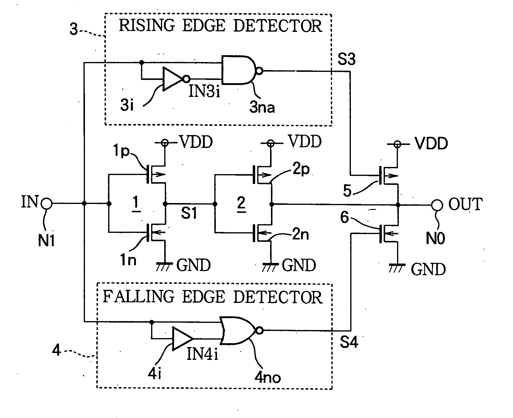
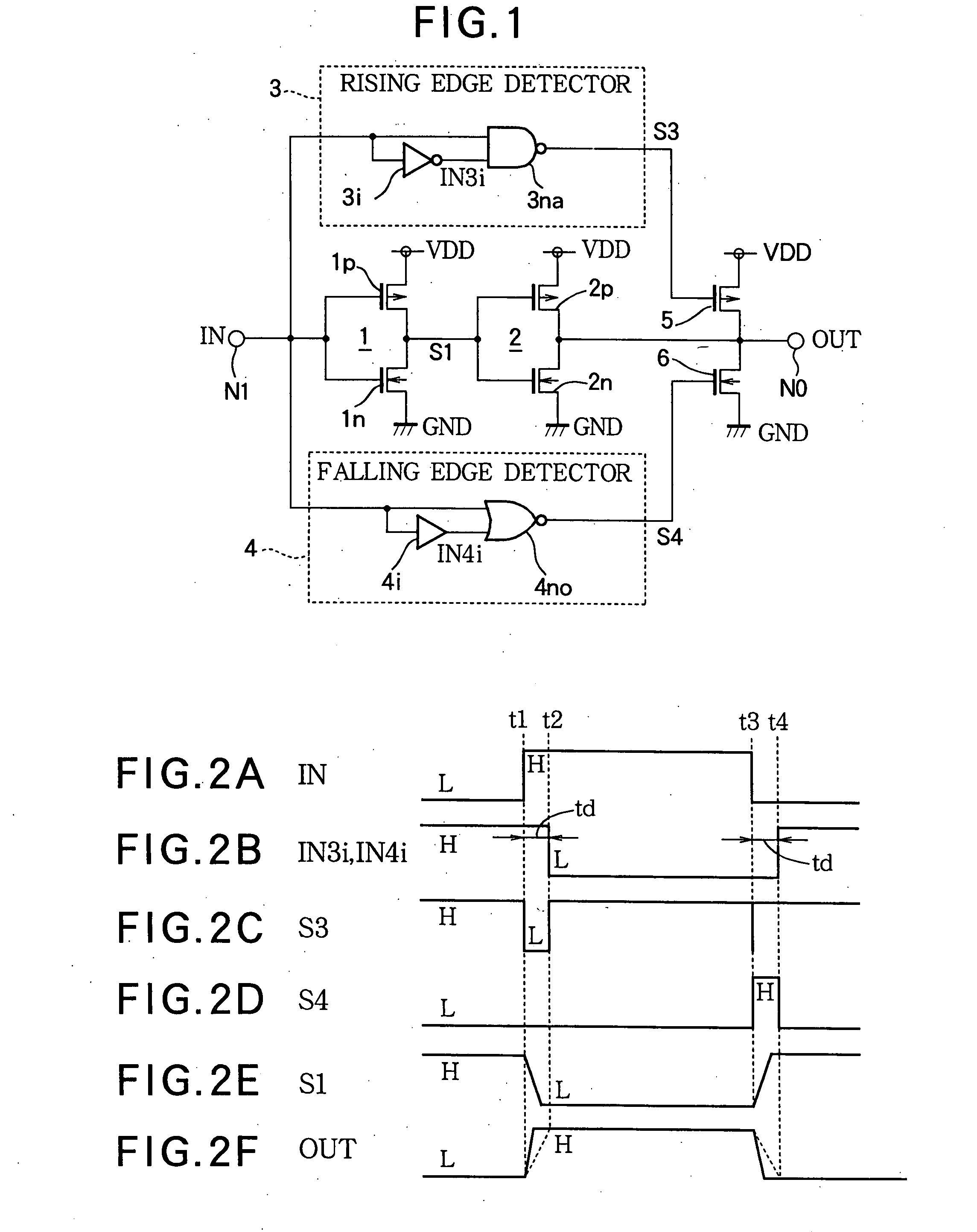
[0039]FIG. 1 shows a driving circuit of Embodiment 1 of the present invention.

[0040]The illustrated circuit includes an input node NI at which an input signal IN is supplied. Connected to the input node NI is a first CMOS inverter 1 comprising a PMOS lp and an NMOS in connected between a power supply potential node VDD and a ground potential node GND.

[0041]Connected to the output side of the CMOS inverter 1 is a second CMOS inverter 2 comprising a PMOS 2p and an NMOS 2n connected between the power supply potential node VDD and the ground potential node GND. The output side of this CMOS inverter 2 is connected to an output node NO, through which the output signal OUT is output. Connected to the input node NI of the driving circuit is a rising edge detector 3 and a falling edge detector 4. The first and the second CMOS inverters 1 and 2 in combination form a driving section for power-amplifying the input signal, and outputting an amplified signal to the output node NO.

[0042]A PMOS 5 i...

Example

Embodiment 2

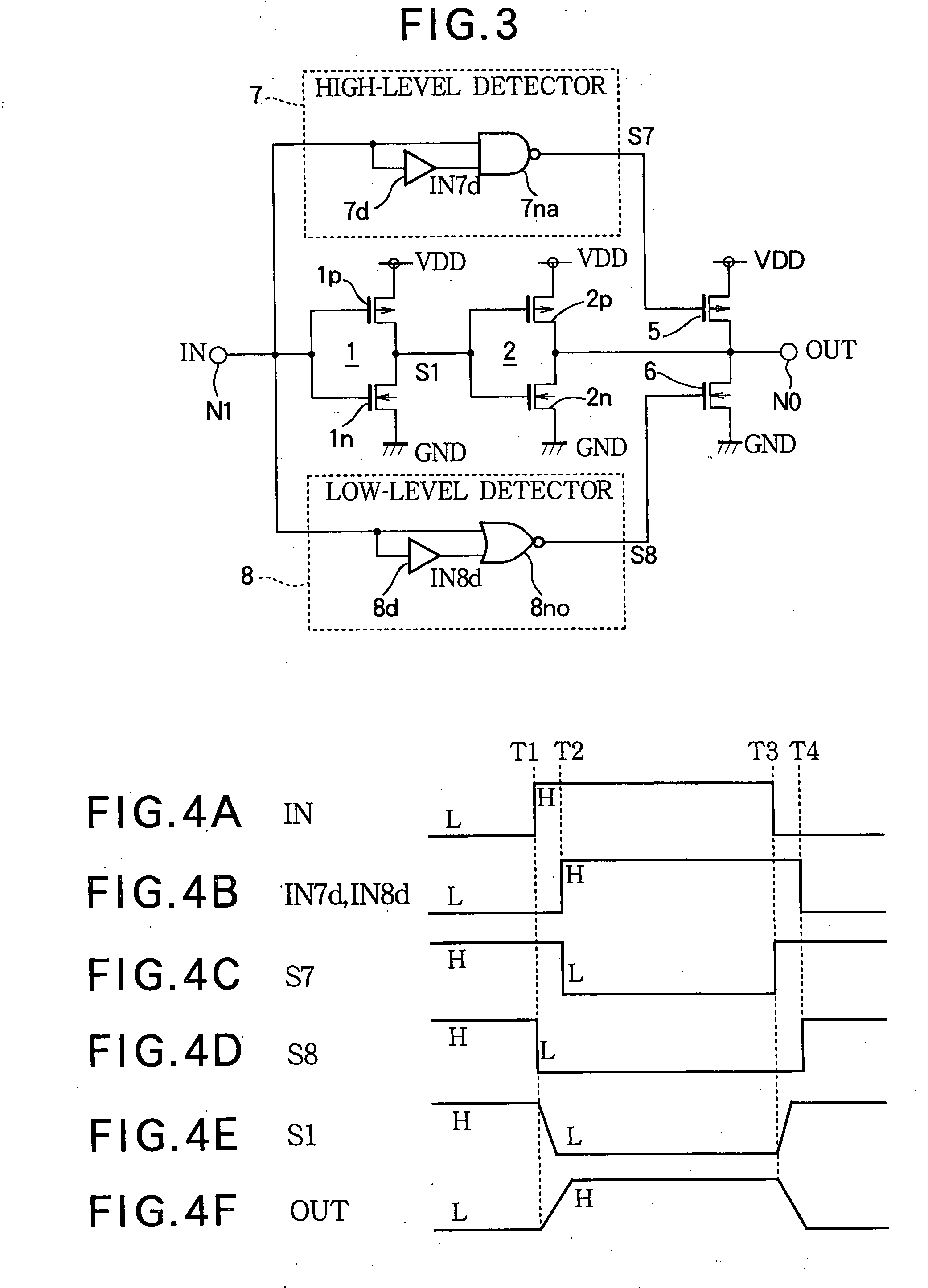
[0059]FIG. 3 shows a driving circuit according Embodiment 2 of the present invention. Reference numerals identical to those in FIG. 1 denote identical or corresponding elements.

[0060]The driving circuit shown in FIG. 3 is provided with a high-level detector 7, serving as a first detector in place of the rising edge detector 3, and a low-level detector 8, serving as a second detector, in place of the falling edge detector 4.

[0061]The high-level detector 7 outputs a high-level detection signal S7 which goes “L” upon expiration of a certain time period after the input signal IN rises from “L” to “H”. When the input signal IN falls from “H” to “L”, the high-level detection signal S7 is returned to “H” instantly. The falling and rising of the high-level detection signal S7 may be described as “commencement” and “termination” of the high-level detection signal S7. The high-level detector 7 comprises a delay element 7d for delaying the input signal IN by a certain time period, ...


PUM


Abstract

In addition to two-stage CMOS inverters for inverting and amplifying the input signal IN, a rising edge detector 3 for detecting the rising edge of the input signal IN, and outputting a rising edge detection signal S3 having a pulse width corresponding to the ambient temperature, and a PMOS 5 for driving the output node NO to the power supply potential VDD according to the rising edge detection signal S3, and the falling edge detector 4 for detecting the falling edge of the input signal IN and outputting a falling edge detection signal S4 having a pulse width corresponding to the ambient temperature, and an NMOS 6 driving the output node NO to the ground potential GND according to the falling edge detection signal S4. When the ambient temperature rises, and the delay time of the CMOS inverters 1, 2 are thereby increased, the pulse widths of the rising edge detection signal S3, and the falling edge detection signal S4 are also increased, and because of the additional driving by means of the PMOS 5 and the NMOS 6, the delay time is reduced. Thus, the variation in the delay time in the driving circuit in an LSI, due to the ambient temperature change can be restrained.

Description

BACKGROUND OF THE INVENTION[0001]The present invention relates a driving circuit (driver) provided in an output stage of an LSI (large-scale integrated circuit) for driving a circuit connected externally to the LSI.[0002]A convention circuit provided in an output stage of an LSI to drive a circuit connected to and provided externally to the LSI, comprises a plurality of stages of CMOS inverters, as described for example in Japanese Patent Kokai Publication No. 2003-133943.[0003]The conventional driving circuit having CMOS inverters has the following problems.(A1) The delay time at each part of the circuit varies with the ambient temperature, causing irregularities with respect to operation timings. In designing an LSI, it was therefore necessary to allow for the variations in the operation timings. However, because of the increase in the size of the LSI, and the miniaturization of each element in the circuit, the variations continue to increase, so that it is becoming more and more ...

Claims


Application Information

Patent Timeline
IPC IPC(8): H03B1/00
CPCH03K5/1534H03K17/04106H03K17/122H03K19/01707H03K17/162H03K17/6872H03K19/00384H03K17/145
Inventor TOKUNO, YOSHIO
Owner LAPIS SEMICON CO LTD
Why Eureka
Try Eureka