
CMOS silicon double-photoelectric detector and manufacturing method thereof

A photodetector, silicon wafer technology, applied in the direction of electric solid devices, circuits, electrical components, etc., can solve the problems of poor short-wave response, the preparation process is not fully compatible with CMOS integrated circuits, etc., achieve good isolation, overcome short-wave response Effects of poor, wide spectral response range

Inactive Publication Date: 2008-02-20
XIAMEN UNIV
View PDF2 Cites 0 Cited by
  • Summary
  • Abstract
  • Description
  • Claims
  • Application Information

AI Technical Summary

Problems solved by technology

[0005] The purpose of the present invention is to provide a silicon photodetector fully compatible with the commercial CMOS industry in view of the shortcomings of the short-wave response of the existing silicon photodetectors, the need to add isolation measures when multiple photodetectors are used, and the preparation process is not fully compatible with CMOS integrated circuits. CMOS silicon double photodetector and its preparation method

Method used


Image

  • CMOS silicon double-photoelectric detector and manufacturing method thereof
  • CMOS silicon double-photoelectric detector and manufacturing method thereof
  • CMOS silicon double-photoelectric detector and manufacturing method thereof

Examples


Embodiment Construction

[0036] The following embodiments will further illustrate the present invention in conjunction with the accompanying drawings.

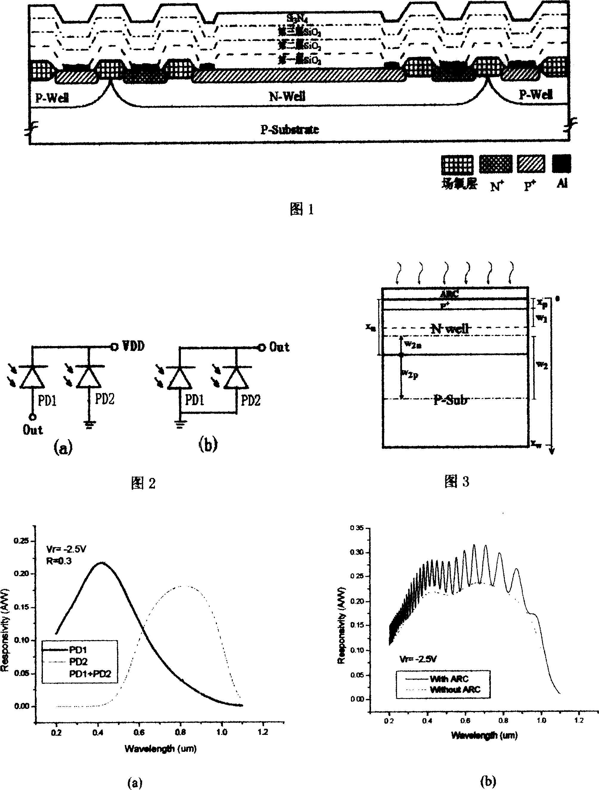
[0037] See Figure 1, in Figure 1, P-Substrate means P-type silicon substrate, N-Well means N well, P-Well means P well, P + Indicates P-type heavy doping, N + Indicates N-type heavy doping, Al indicates metal aluminum, SiO 2 Indicates the surface insulating dielectric layer (a total of 3 layers from bottom to top in the order of preparation), Si 3 N 4 Indicates the surface passivation layer.

[0038] The CMOS silicon dual photodetector shown in Figure 1 contains two photodetectors with a PN structure: P + / N-well and N-well / P-sub, respectively called PD1 and PD2, where Al and N + An ohmic contact is formed as the cathode of the detector, the cathodes of PD1 and PD2 are common in this configuration. P in the N-well + A1 in contact with it forms an ohmic contact as the anode of PD1; P in the P well + The Al in contact with it forms an ohmic cont...


PUM


Abstract

A CMOS silicon twin photo detector is prepared as setting p type of silicon substrate, N well, p well, p type of heavy doped silicon and N type of heavy doped silicon on the same silicon wafer; using silicon oxide generated on silicon wafer surface by oxidation as field oxide; depositing metal aluminum on silicon wafer surface through sputtering process, attaching SiO2 insulation media layer on silicon substrate by deposition process and attaching Si3N4 surface passivation layer on SiO2 insulation media layer by deposition process.

Description

technical field [0001] The invention relates to a photoelectric integrated circuit, in particular to a CMOS silicon photodetector. Background technique [0002] In recent years, silicon photodetectors have developed rapidly and have been widely used, especially in the fields of optical fiber communication, optical disk system, photoelectric measurement and so on. For example, it can be used for performance testing of optical pickup heads, barcode readers, and VLSI circuits of DVDs and CD-ROMs. In the field of optical fiber communication, silicon-based photodetectors have been used in 850nm optical fiber communication and 650nm plastic optical fiber communication. These all depend on the spectral characteristics determined by the silicon material itself. On the other hand, silicon-based photodetectors can be realized by silicon integrated circuit technology, and can be easily integrated with silicon IC circuits with various functions to realize monolithic integrated optoele...

Claims


Application Information

Patent Timeline
Patent Type & Authority Patents(China)
IPC IPC(8): H01L27/14
Inventor 陈朝卞剑涛
Owner XIAMEN UNIV
Learn More