Photoelectric sensor integrated chip for smart home

A photoelectric sensor and integrated chip technology, applied in the field of photoelectric sensors, can solve the problems that electrical signals are easily affected by the outside world, the package size cannot be further reduced, and input data errors, etc., to overcome poor short-wave response and large junction capacitance. , the effect of increased bandwidth

Active Publication Date: 2017-04-05
XIAMEN UNIV
View PDF5 Cites 0 Cited by
  • Summary
  • Abstract
  • Description
  • Claims
  • Application Information

AI Technical Summary

Problems solved by technology

Since the converted electrical signal is very weak, it is extremely vulnerable to external influences, resulting in input data errors
In addition, some integrated photoelectric sensors, such as infrared remote control receivers, use the method of directly binding two gold wires from the photodiode to the amplifier circuit, and then package the two together. Although the risk of interference can be greatly reduced, but Need to add a bonding process, increase the cost and risk of unreliable bonding, and the package size cannot be further reduced

Method used


Image

  • Photoelectric sensor integrated chip for smart home
  • Photoelectric sensor integrated chip for smart home
  • Photoelectric sensor integrated chip for smart home

Examples


Embodiment Construction

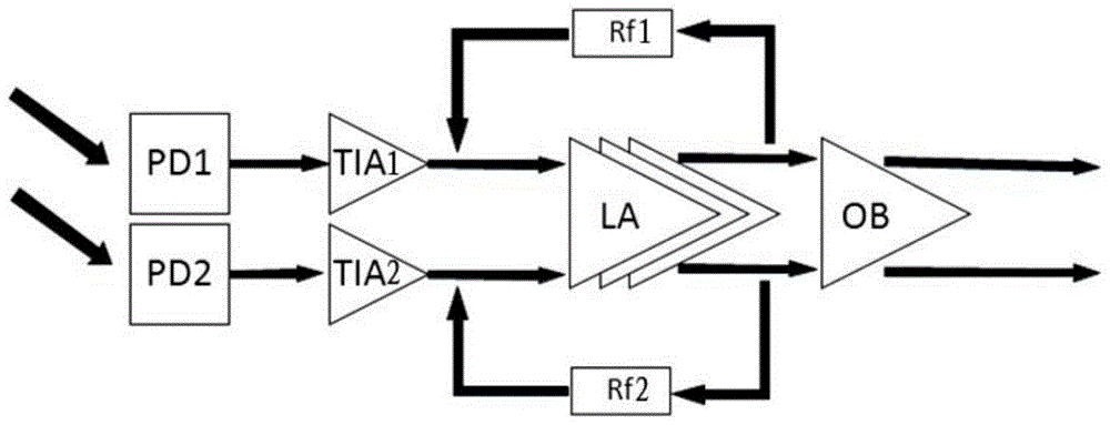
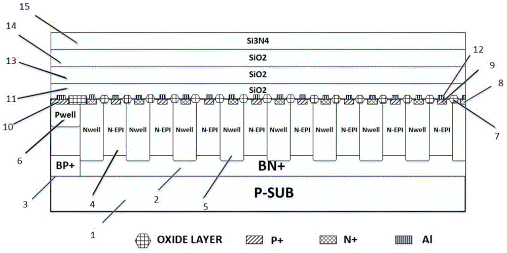
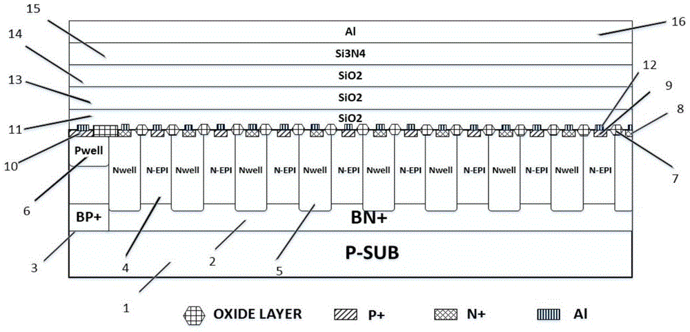
[0026] The silicon-based monolithic optoelectronic integrated receiving chip described in the embodiment of the present invention is manufactured by a 0.5 μm standard BCD process, and is equipped with a silicon-based photodetector and a corresponding preamplifier circuit.

[0027] see figure 1 , the embodiment of the present invention is provided with the first silicon-based photodetector PD1, the first transimpedance preamplifier TIA1, the first DC negative feedback circuit Rf1, the second silicon-based photodetector PD2, the second mutual Resistance preamplifier TIA2, the second DC negative feedback circuit Rf2, limiting amplifier LA, output buffer circuit OB.

[0028] The output terminal of the first silicon-based photodetector PD1 is connected to the input terminal of the first transimpedance preamplifier TIA1, and the output terminal of the first transimpedance preamplifier TIA1 is connected to the first differential input terminal of the limiting amplifier LA, The outpu...


PUM


Abstract

A photoelectric sensing integrated chip applied to smart home relates to photoelectric sensors. The photoelectric sensing integrated chip is provided with a first silicon-based photoelectric detector, a first transimpedance preamplifier, a first DC negative feedback circuit, a second silicon-based photoelectric detector, a second transimpedance preamplifier, a second DC negative feedback circuit, an amplitude limiting amplifier, and an output buffer circuit; wherein an output end of the first silicon-based photoelectric detector is connected with an input end of the first transimpedance preamplifier, an output end of the first transimpedance preamplifier is connected with a first differential input end of the amplitude limiting amplifier, an output end of the second silicon-based photoelectric detector is connected with an input end of the second transimpedance preamplifier, an output end of the second transimpedance preamplifier is connected with a second differential input end of the amplitude limiting amplifier, an output end of the amplitude limiting amplifier is connected with an input end of the output buffer circuit, an output end of the output buffer circuit is connected with an external circuit; the output ends of the amplitude limiting amplifier are connected with the two differential input ends of the amplitude limiting amplifier respectively through the first DC negative feedback circuit and the second DC negative feedback circuit.

Description

technical field [0001] The invention relates to a photoelectric sensor, in particular to a photoelectric sensor integrated chip applied to smart home. Background technique [0002] With the improvement of living standards, people's requirements for high-efficiency and convenient home furnishing are becoming more and more significant, and home automation, informatization, and intelligence will become the mainstream trend. In recent years, with the high development of informatization, the liberalization and high-level of communication, the rapid increase of business volume and the improvement of human's requirements for energy saving, safety, comfort and efficiency of living environment, the demand for smart home is more significant ( Chinese patent CN201410571226.7). In order to achieve intelligence, the input signals such as sound, light, and electricity from the outside world must first be converted into electrical signals that the central processing unit can recognize, an...

Claims


Application Information

Patent Timeline
Patent Type & Authority Patents(China)
IPC IPC(8): G01J1/42
Inventor 程翔楼卓格颜黄苹范程程郑明徐攀
Owner XIAMEN UNIV
Why Eureka
Try Eureka