Pixel circuit and display apparatus

A pixel circuit and display device technology, which is applied in the field of pixel circuits and display devices, can solve problems such as the reduction of aperture ratio, the change of peripheral circuits driving pixel circuits, and the increase in the number of pixel circuit components, so as to achieve high aperture ratio and improve configuration freedom Effect

Active Publication Date: 2008-09-17
SANYO ELECTRIC CO LTD
View PDF6 Cites 2 Cited by
  • Summary
  • Abstract
  • Description
  • Claims
  • Application Information

AI Technical Summary

Problems solved by technology

[0011] However, in this scheme, it is necessary to set up a circuit for compensating for threshold variation
Therefore, if such a circuit is used, the number of components of the pixel circuit increases and the aperture ratio becomes smaller.
In addition, when adding a circuit for compensation, there will be a problem that the peripheral circuit for driving the pixel circuit must be changed.

Method used


Image

  • Pixel circuit and display apparatus
  • Pixel circuit and display apparatus
  • Pixel circuit and display apparatus

Examples


Embodiment Construction

[0073] Hereinafter, embodiments of the present invention will be described with reference to the drawings.

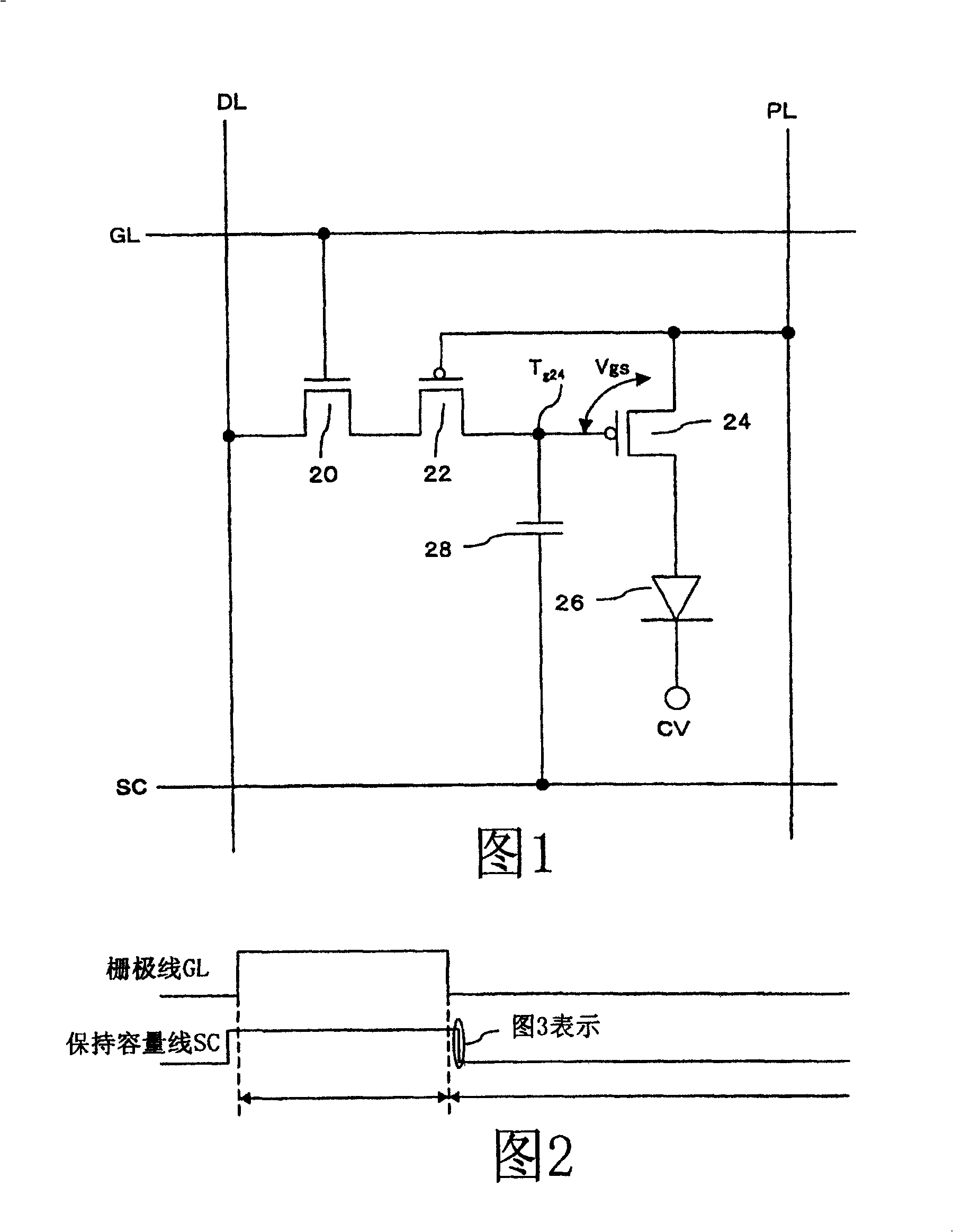
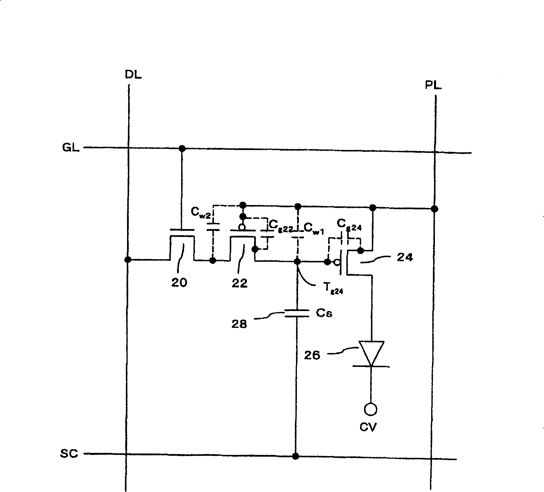
[0074] FIG. 1 is a diagram showing a pixel circuit configuration of one pixel according to the embodiment. The first conductive region (drain) of the n-type channel selection TFT 20 is connected to the data line DL extending in the vertical scanning direction. The gate (control end) of the selection TFT 20 is connected to the gate line GL extending in the horizontal scanning direction, and the second conductive region (source) is connected to the first conductive region (source) of the p-type channel correction TFT 22. . In addition, the selection TFT 20 may also be a p-type channel, and if it is a p-type channel, the polarity (H potential or L potential) of the selection signal (gate signal) output to the gate line GL should be reversely driven. You can.

[0075] The control terminal (gate) of the correction TFT 22 is connected to the power supply line PL (voltage P...


PUM


Abstract

A selecting TFT (20) and a correcting TFT (22) are turned on, thereby causing a data voltage on a data line to be held, as a gate voltage of a driving TFT (24), by a hold capacitor (28). After the selecting TFT (20) is turned off, the voltage of a capacitance line (SC) is caused to rise, thereby turning on the driving TFT (24) to cause a driving current to flow through an organic EL element (26). Here, the correcting TFT (22) is on before the rise of the capacitance line (SC), while it is turned off at a midpoint during the fall of the capacitance line (SC). Accordingly, the capacitance value of the correcting TFT (22) varies during the rise of the gate voltage, and the slope of the rise of the gate voltage of the driving TFT (24) varies, whereby the gate voltage after a fall of the capacitance line (SC) can be set in accordance with the variation of the threshold value of the driving TFT (24). Particularly, the driving TFT (24) and the correcting TFT (22) are disposed such that they are adjacent to each other, whereby their characteristics can be treated as the same and hence the correction can be effectively performed.

Description

technical field [0001] The present invention relates to a pixel circuit including a light-emitting element such as an organic EL (Electro Luminescence) element, and a display device in which the organic EL element is arranged in a matrix. Background technique [0002] An organic EL panel using an organic EL element as a light-emitting element is known, and its development is progressing. In this organic EL panel, organic EL elements are arranged in a matrix, and light emission of the organic EL elements is individually controlled to perform display. In particular, in an active matrix organic EL panel, each pixel has a TFT for controlling display, and by controlling the operation of the TFT, the light emission of each pixel can be controlled, so that very high-precision display can be performed. [0003] Figure 13 What is shown is an example of a pixel circuit of an active matrix organic EL panel. A data line supplying a data voltage for displaying pixel luminance is conne...

Claims


Application Information

Patent Timeline
Patent Type & Authority Patents(China)
IPC IPC(8): G09G3/30G09G3/20
Inventor 古河雅行丸毛浩二
Owner SANYO ELECTRIC CO LTD
Why Eureka
Try Eureka