
Organicelectroluminescent device and its preparation method

An electroluminescent device, organic technology, applied in the direction of electroluminescent light source, electric solid-state device, semiconductor/solid-state device manufacturing, etc., can solve the problems of large doping concentration error of the light-emitting layer, unstable device performance, and can no longer be adjusted. , to achieve the effect of good stability and luminous performance

Inactive Publication Date: 2008-10-15
TSINGHUA UNIV +1
View PDF4 Cites 0 Cited by
  • Summary
  • Abstract
  • Description
  • Claims
  • Application Information

AI Technical Summary

Problems solved by technology

However, when the dopant concentration is required to be lower than 0.01 mole percent, the doping concentration error of the light-emitting layer prepared by pre-doping is also quite large, resulting in unstable device performance
Also, once the pre-mixed dopant-prehost material ratio is fixed, it cannot be adjusted during the evaporation process

Method used


Image

  • Organicelectroluminescent device and its preparation method
  • Organicelectroluminescent device and its preparation method
  • Organicelectroluminescent device and its preparation method

Examples


Embodiment 1

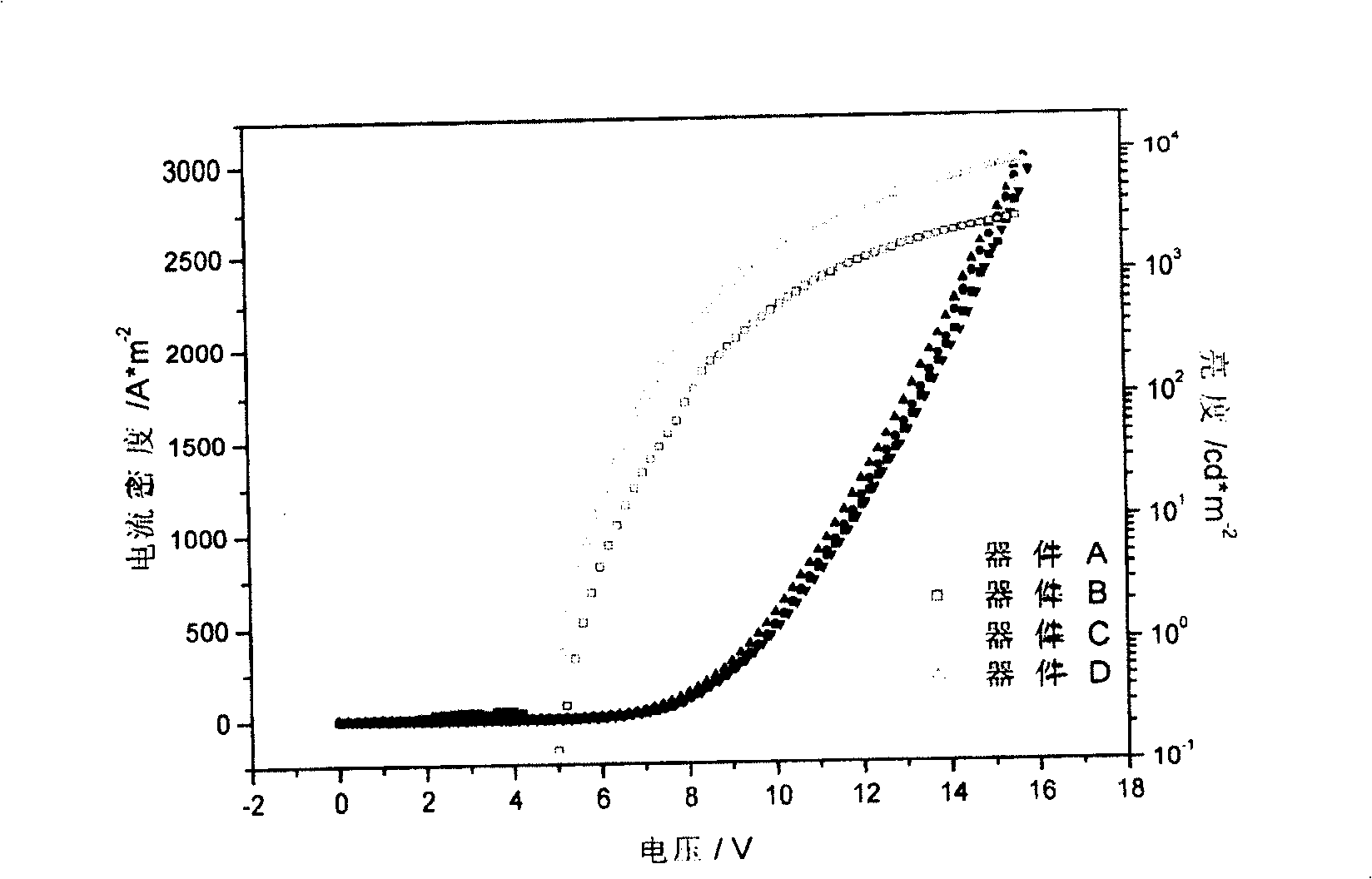
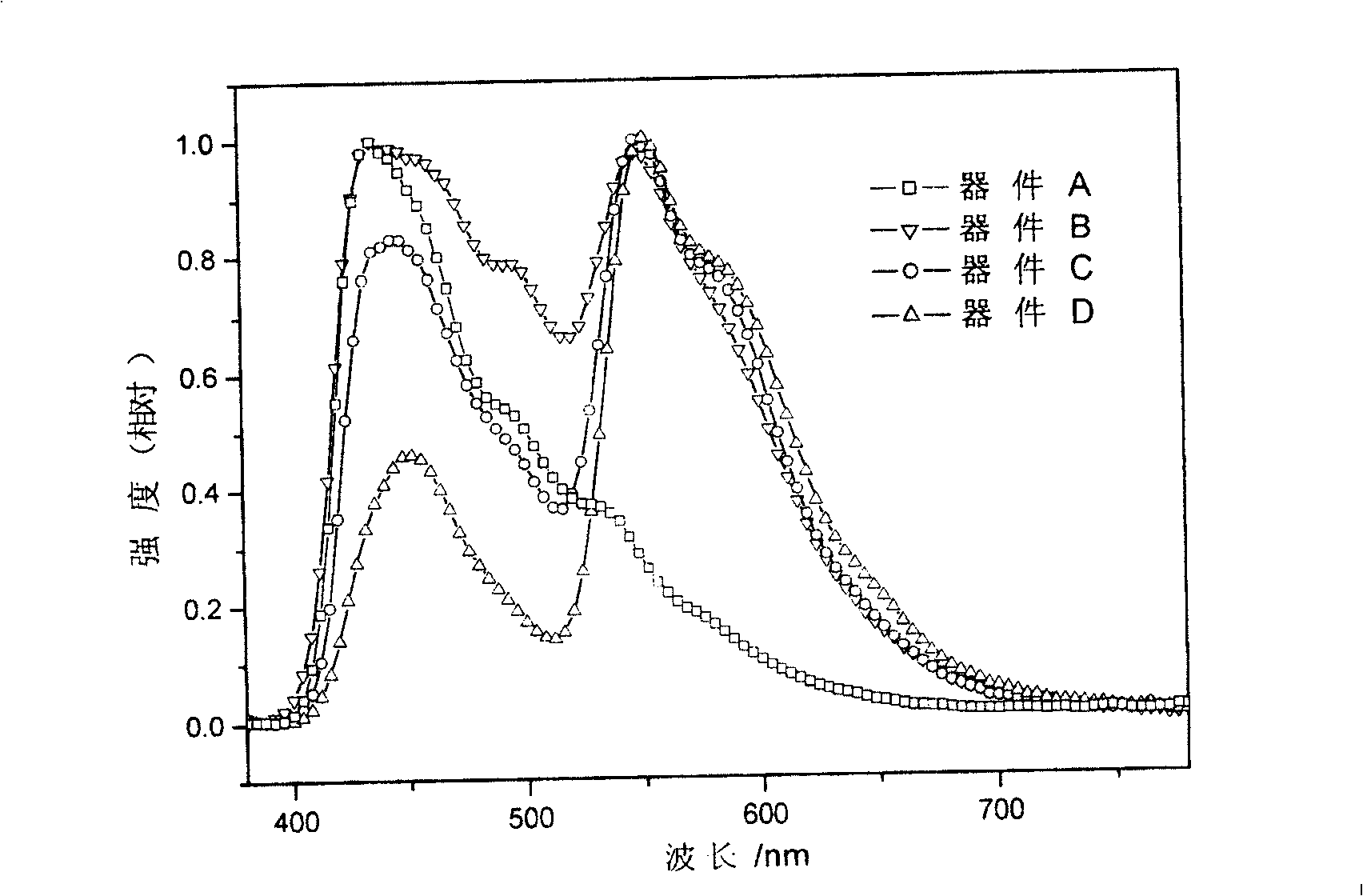
[0053] Embodiment 1: Preparation of organic electroluminescence device OLED-1 (A-D)

[0054] The glass plate coated with the transparent conductive layer of indium tin oxide is ultrasonically treated in a commercial cleaning agent, rinsed in deionized water, ultrasonically degreased in acetone: ethanol mixed solvent, and baked in a clean environment until the water is completely removed , irradiated with a UV light cleaner for 10 minutes, and bombarded the surface with a low-energy positive ion beam.

[0055] A 50 nm thick 4,4'-bis[1-naphthyl]-N-anilino]-biphenyl hole transport layer was deposited on indium tin oxide by thermal evaporation.

[0056] Mix solid material 99% 99% 9,9,10-bis(2-naphthyl)anthracene and 1% rubrene according to molar percentage, then melt the mixture in a container with a chemically inert environment, cool to room temperature, and take it out from the container Uniform pre-doped luminescent material, put it into evaporation source 1, put 9,9,10-bis(2-...

Embodiment 2

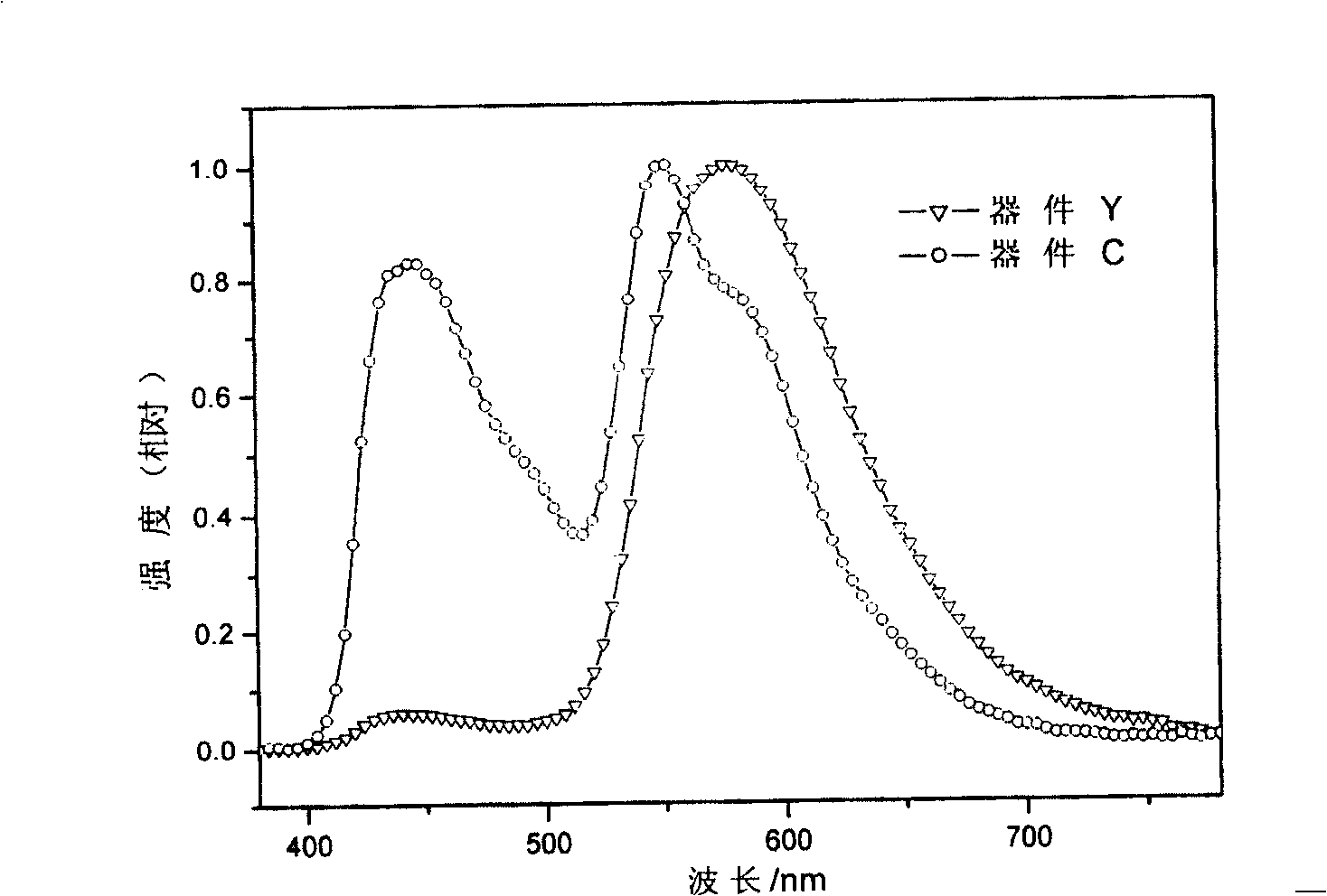
[0067] The glass plate coated with the transparent conductive layer of indium tin oxide is ultrasonically treated in a commercial cleaning agent, rinsed in deionized water, ultrasonically degreased in acetone: ethanol mixed solvent, and baked in a clean environment until the water is completely removed , irradiated with a UV light cleaner for 10 minutes, and bombarded the surface with a low-energy positive ion beam.

[0068] A 50 nm thick 4,4'-bis[1-naphthyl]-N-anilino]-biphenyl hole transport layer was deposited on indium tin oxide by thermal evaporation.

[0069] Mix solid material 99% 99% 9,9,10-bis(2-naphthyl)anthracene and 1% rubrene according to molar percentage, then melt the mixture in a container with a chemically inert environment, cool to room temperature, and take it out from the container Uniform pre-doped luminescent material, put it into evaporation source 1, put 9,9,10-bis(2-naphthyl)anthracene in evaporation source 2, control the evaporation rate of evaporatio...

Embodiment 3

[0075] Embodiment 3: Preparation of organic electroluminescent device OLED-2 (A-D)

[0076] The glass plate coated with the transparent conductive layer of indium tin oxide is ultrasonically treated in a commercial cleaning agent, rinsed in deionized water, ultrasonically degreased in acetone: ethanol mixed solvent, and baked in a clean environment until the water is completely removed , irradiated with a UV light cleaner for 10 minutes, and bombarded the surface with a low-energy positive ion beam.

[0077] A 50 nm thick 4,4'-bis[1-naphthyl]-N-anilino]-biphenyl hole transport layer was deposited on indium tin oxide by thermal evaporation.

[0078] Mix solid material 99% 2-tert-butyl-9,10-bis(2-naphthyl)anthracene and 1% rubrene according to molar percentage, then melt the mixture in a container with a chemically inert environment, cool to room temperature, Take out the uniform pre-doped luminescent material from the container, put it into evaporation source 1, put 9,9,10-di(...


PUM


Abstract

Luminescent layer of the device includes at least one organic main body material and at least one adulterant. Adulterant is 0.1ppm - 500ppm (mole) of main body material. The device can realizes modulations of light color or hue and luminous efficiency without influence on current and voltage characteristics of main body material. The device possesses better stability and luminescence. In the invention, the device is prepared through mixing doping method by using doping in advance and coating by vaporization with double sources. Comparing with prior art, the invention controls doping density of adulterant accurately. More over, evaporation rate of double sources can be controlled in procedure of coating by vaporization to adjust density of adulterant through more means. Thus, the invention is flexible.

Description

technical field [0001] The invention relates to an organic electroluminescence device and a preparation method thereof. Background technique [0002] Today, with the development of multimedia technology and the advent of the information society, the requirements for the performance of flat panel displays are getting higher and higher. Three new display technologies emerging in recent years: plasma display, field emission display and organic light emitting device (OLED), all make up for the shortcomings of cathode ray tubes and liquid crystal displays to a certain extent. Among them, OLED has a series of advantages such as self-illumination, low-voltage DC drive, full curing, wide viewing angle, and rich colors. Compared with liquid crystal displays, OLED does not require a backlight source, has a large viewing angle, low power, and its response speed is faster than that of liquid crystal displays. 1000 times higher than that of a liquid crystal display with the same resolut...

Claims


Application Information

Patent Timeline
Patent Type & Authority Patents(China)
IPC IPC(8): H05B33/12H01L51/52H01L51/56H05B33/14H05B33/10
Inventor 邱勇段炼王立铎
Owner TSINGHUA UNIV
Learn More