Synchronous mirror delay (SMD) circuit and method including a ring oscillator for timing coarse and fine delay intervals

A delay circuit, fine delay technology, applied in the direction of electrical components, automatic power control, signal generation/distribution, etc., can solve the problem of SMD power consumption and so on

Inactive Publication Date: 2008-11-05
MICRON TECH INC
View PDF4 Cites 2 Cited by
  • Summary
  • Abstract
  • Description
  • Claims
  • Application Information

AI Technical Summary

Problems solved by technology

Also, these large numbers of individual delay stages 110A-N, 116A-N can result in significant power consumption of the SMD 100, which may not be desirable, especially if the synchronous storage device is included in a portable battery powered device

Method used


Image

  • Synchronous mirror delay (SMD) circuit and method including a ring oscillator for timing coarse and fine delay intervals
  • Synchronous mirror delay (SMD) circuit and method including a ring oscillator for timing coarse and fine delay intervals
  • Synchronous mirror delay (SMD) circuit and method including a ring oscillator for timing coarse and fine delay intervals

Examples


Embodiment Construction

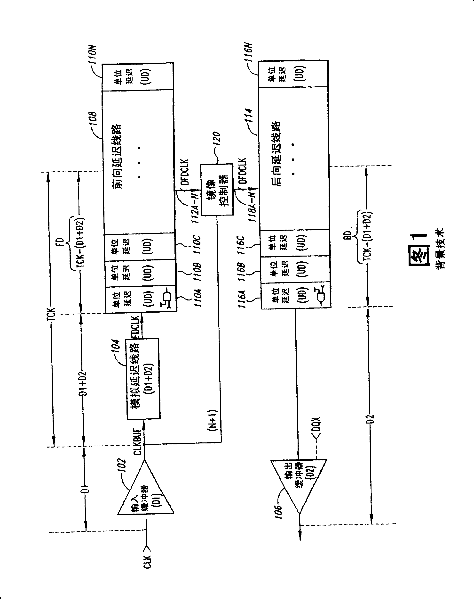
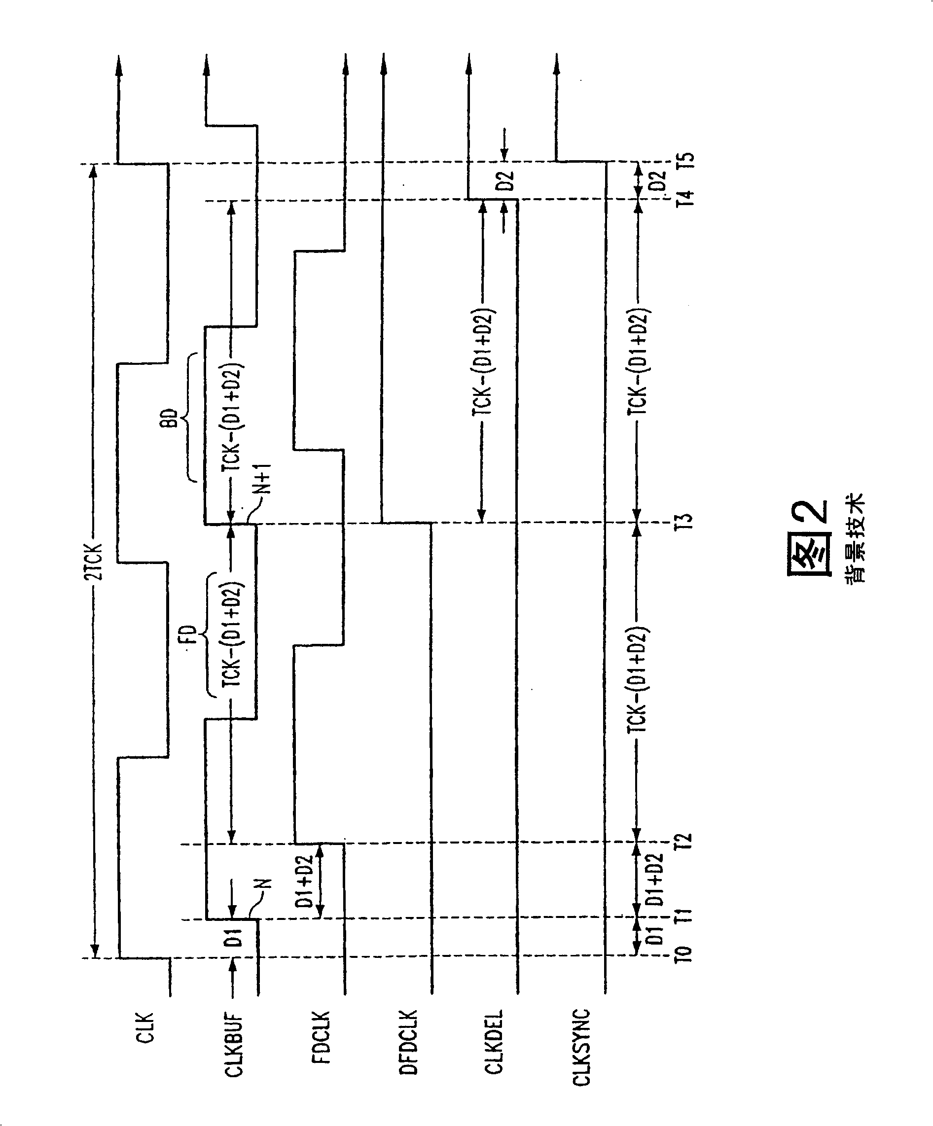
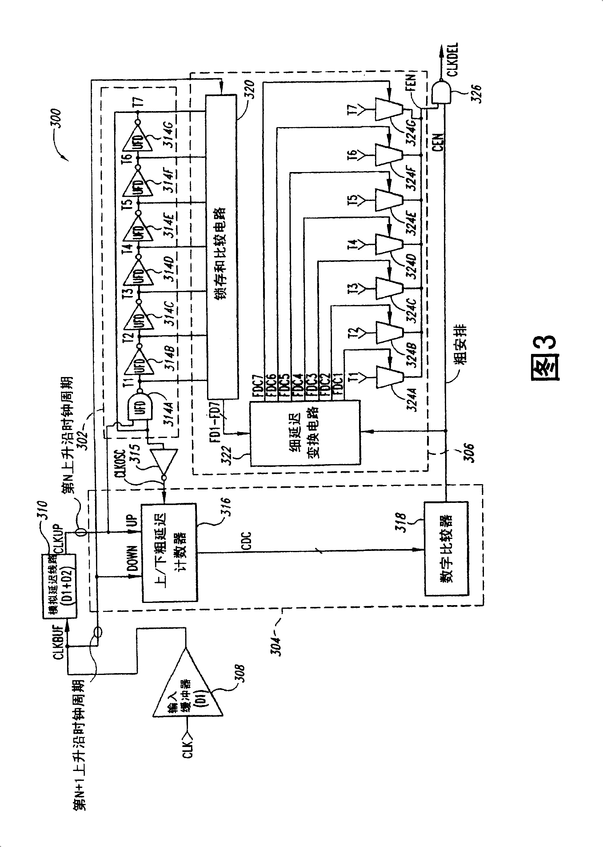
[0024] FIG. 3 is a functional block diagram of the rising edge portion of the SMD 300, in which the SMD 300 removes the relatively large and high-power forward and backward delay lines 108 included in the conventional SMD 100 described in FIG. 1, and replaces it A ring oscillator 302 is included. The ring oscillator 302 provides a clock to the coarse delay circuit 304 to define a coarse delay CD, and is utilized by the fine delay circuit 306 to define a fine delay FD. During operation, the SMD 300 adjusts the values ​​of the coarse and fine delays CD and FD to generate a delayed clock signal CLKDEL that is synchronized with the external clock signal CLK (for example, has a desired delay relative to the external clock signal), as will be described in more detail below . In the following description, specific details are explained to provide a thorough understanding of the present invention. However, it is obvious to a person of ordinary skill in the art that the present invention c...


PUM


Abstract

A synchronous mirror delay (300) includes a ring oscillator that generates a plurality of tap clock signals (T1-T7) with one tap clock signal being designated an oscillator clock signal. In response to an input clock signal, a model delay line generates a model delayed clock signal having a model delay relative to the input clock signal. A coarse delay circuit generates a coarse delay count (316) responsive to the oscillator, input, and model delayed clock signals, and activates a coarse delay enable signal responsive to the delay count being equal to a reference count value. A fine delay circuit latches the tap clock signals and develops a fine delay from the latched signals, and activates a fine delay enable signal having the fine delay in response to the coarse delay enable signal. An output circuit generates a delayed clock signal responsive to the coarse and fine delay enable signals going active.

Description

Technical field [0001] The present invention relates generally to integrated circuits, and more specifically, to synchronizing an internal clock signal generated in an integrated circuit with an external clock signal applied to the integrated circuit. Background technique [0002] In a synchronous integrated circuit, the integrated circuit is clocked by an external clock signal and performs operations at a predetermined time, wherein the predetermined time is related to the rising and falling edges of the applied clock signal. Examples of synchronous integrated circuits include synchronous storage devices, such as synchronous dynamic random access memory (SDRAM), synchronous static random access memory (SSRAM), and cassette memory such as SLDRAM and RDRAM, as well as other types of integrated circuits , For example, a microprocessor. The timing of synchronizing the external signal of the storage device is determined by the external clock signal, and it is usually necessary to syn...

Claims


Application Information

Patent Timeline
Patent Type & Authority Patents(China)
IPC IPC(8): H03L7/00G06F1/10G11C7/10G11C7/22G11C11/407H03K5/00H03K5/135
CPCG11C7/22G11C7/222H03K5/135H03L7/00H03B1/00H03B27/00
Inventor 霍华德·C·基尔希
Owner MICRON TECH INC
Why Eureka
Try Eureka