Liquid-crystal display panel and its production

A technology of liquid crystal display panel and manufacturing method, which is applied in semiconductor/solid-state device manufacturing, transistors, static indicators, etc., can solve the problems of misalignment between the upper substrate 130 and the lower substrate 110, abnormal image display, etc., and solve the problem of abnormal display images normal effect

Inactive Publication Date: 2008-11-12
高智发明基金第82有限责任公司
View PDF11 Cites 0 Cited by
  • Summary
  • Abstract
  • Description
  • Claims
  • Application Information

AI Technical Summary

Problems solved by technology

In addition, since the spacer 102 is in complete contact with the contact surface of the lower substrate 110 and there is no solidified layer between the two, when the liquid crystal display panel 100 is subjected to an external lateral force F, it is easy to cause the upper substrate 130 to contact the lower substrate 110. Relative misalignment, resulting in abnormal image display

Method used


Image

  • Liquid-crystal display panel and its production
  • Liquid-crystal display panel and its production
  • Liquid-crystal display panel and its production

Examples


Embodiment Construction

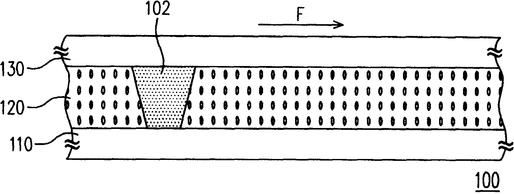
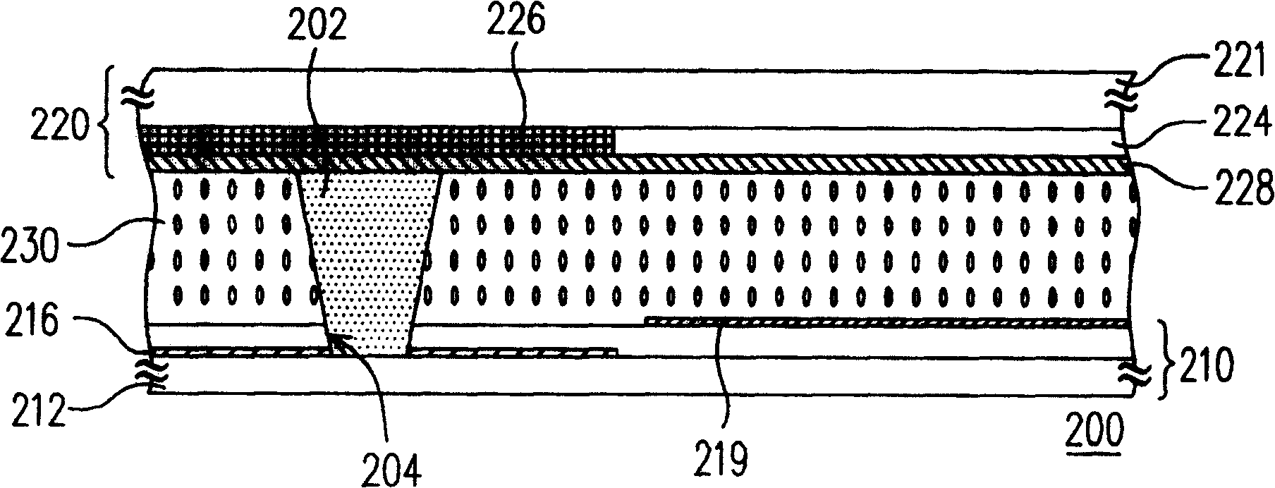
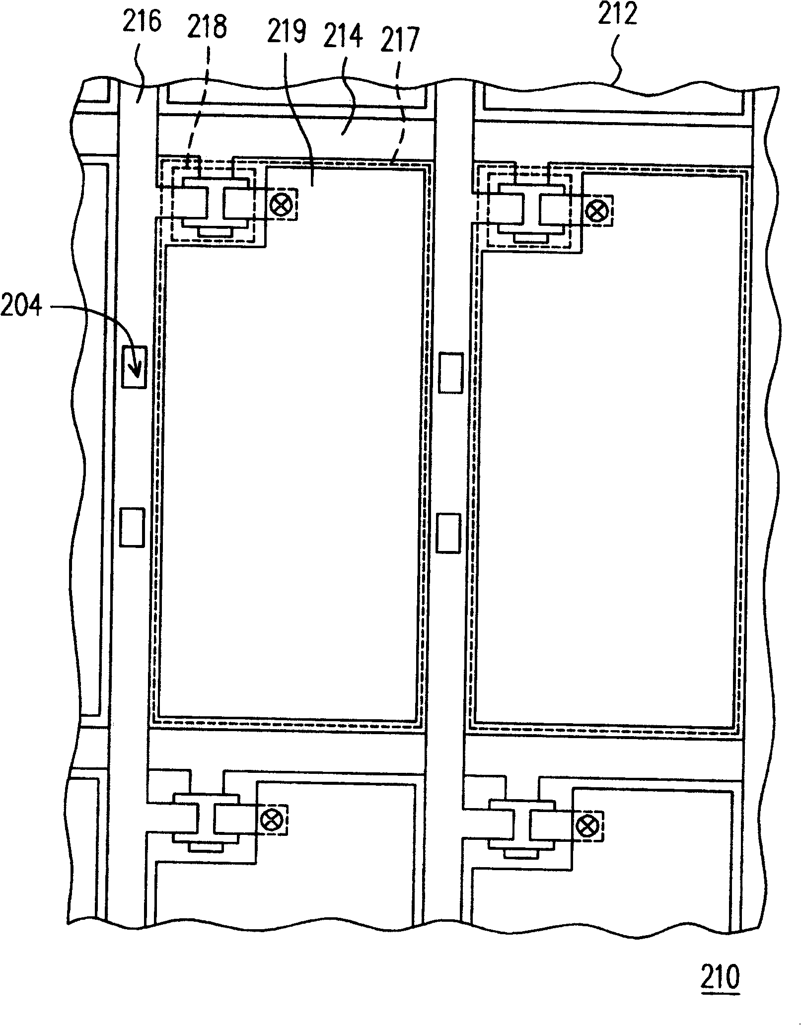
[0053] figure 2 It is a schematic cross-sectional view of a liquid crystal display panel in a preferred embodiment of the present invention. image 3 then figure 2 A partial top view of the active device array 210 shown in FIG. Please also refer to figure 2 and image 3 , the liquid crystal display panel 200 is mainly composed of an active device array 210 , a front substrate 220 , a first spacer 202 and a liquid crystal layer 230 . Wherein, the active element array 210 is a thin film transistor array (thin film transistor array, TFT array), which is composed of a substrate 212, a plurality of scanning lines 214, a plurality of data lines 216, a plurality of active elements 218 and a plurality of pixel electrodes 219 constituted. The scan wires 214 and the data wires 216 are disposed on the substrate 212 , and a plurality of pixel regions 217 are defined on the substrate 212 .

[0054] Please continue to refer to figure 2 and image 3, the data wiring 216 has the o...


PUM

PropertyMeasurementUnit
depthaaaaaaaaaa

Abstract

A liquid crystal front plate is prepared as laying base plate above active element array, setting the first space block between front base plate and active element array as the first space block being embedded in opening on active element array partially and setting liquid crystal layer between active element array and front base plate.

Description

technical field [0001] The invention relates to a display device and a manufacturing method thereof, and in particular to a liquid crystal display panel and a manufacturing method thereof. Background technique [0002] The rapid progress of the multimedia society is largely due to the rapid progress of semiconductor components and display devices. As far as displays are concerned, thin film transistor liquid crystal displays (Thin FilmTransistor Liquid Crystal Display, TFT LCD) with superior characteristics such as high image quality, good space utilization efficiency, low power consumption, and no radiation have gradually become the mainstream of the market. [0003] figure 1 It is a schematic cross-sectional view of a known liquid crystal display panel. Please refer to figure 1 The liquid crystal display panel 100 is composed of a lower substrate 110 , a liquid crystal layer 120 and an upper substrate 130 . Wherein, the liquid crystal layer 120 is sealed between the lo...

Claims


Application Information

Patent Timeline
Patent Type & Authority Patents(China)
IPC IPC(8): G02F1/133G02F1/1335G02F1/136H01L29/786H01L21/027G09F9/35
Inventor 李明书
Owner 高智发明基金第82有限责任公司
Why Eureka
Try Eureka