
Mending system and method of spot zone of flat plate display

A flat-panel display and bright spot technology, which is applied to instruments, nonlinear optics, optics, etc., can solve problems such as reducing the intensity of the flat-panel display 1, breaking the filter substrate 13, and shortening the service life of the flat-panel display 1.

Active Publication Date: 2008-11-26
METAL INDS RES & DEV CENT
View PDF8 Cites 0 Cited by
  • Summary
  • Abstract
  • Description
  • Claims
  • Application Information

AI Technical Summary

Problems solved by technology

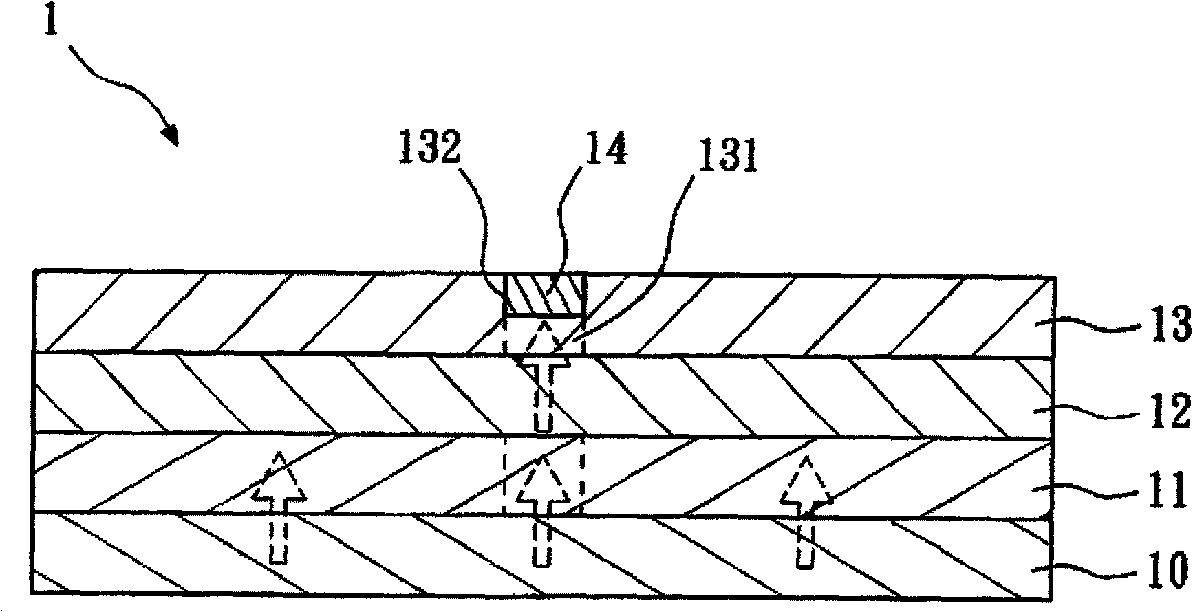
[0004] The conventional method of repairing the bright spot area of ​​a flat panel display must form a cavity 132 in the bright spot area 131 on the filter substrate 13, thus easily causing the problem of cracking of the filter substrate 13
Furthermore, filling the jelly-like substance 14 in the cavity 132 requires another post-cleaning action, and it is easy to cause falling off after long-term use.
To sum up the above, the conventional method of repairing the bright spot area of ​​the flat panel display is likely to cause the filter substrate 13 to be broken, which will reduce the strength of the flat panel display 1 and shorten the service life of the flat panel display 1

Method used


Image

  • Mending system and method of spot zone of flat plate display
  • Mending system and method of spot zone of flat plate display
  • Mending system and method of spot zone of flat plate display

Examples


Embodiment Construction

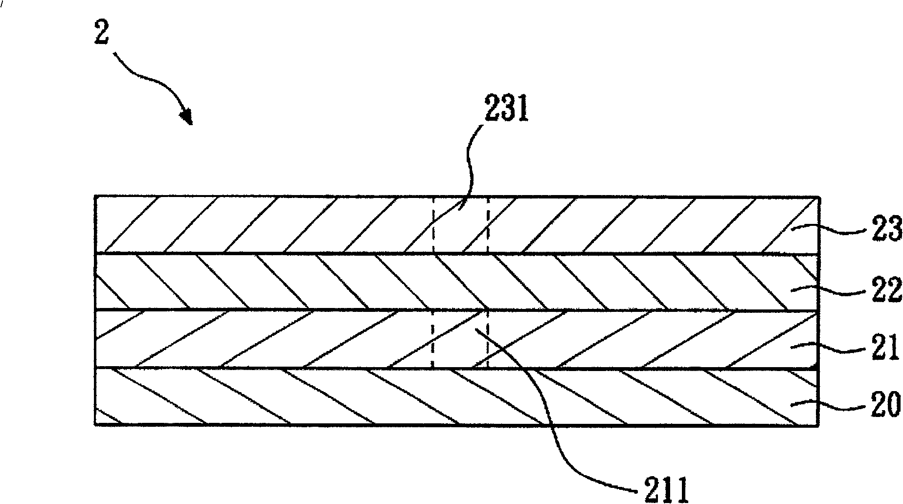
[0018] refer to image 3 , which shows a schematic diagram of the flat panel display of the present invention. The flat panel display 2 has a backlight module 20 , a TFT substrate 21 , a liquid crystal layer 22 and a filter substrate 23 . The thin film transistor substrate 21 is disposed on the backlight module 20 , the liquid crystal layer 22 is disposed on the thin film transistor substrate 21 , and the filter substrate 23 is disposed on the liquid crystal layer 22 . The TFT substrate 21 has at least one light-transmitting region 211 , and the light-transmitting region 211 cannot shield the light generated by the backlight module 20 . The filter substrate 23 has at least one bright spot area 231 , and the bright spot area 231 is at a position corresponding to the transparent area 211 .

[0019] refer to Figure 4 , which shows a schematic diagram of the method for repairing the bright spot area of ​​a flat panel display according to the present invention. First, a target...


PUM

PropertyMeasurementUnit
thicknessaaaaaaaaaa

Abstract

The present invention relates to a system and a method for repairing the bright spot area of the flat panel display. Said method contains: (a) mounting the target material on the flat panel display which has one bright spot at least on the surface, the said target material has a metallic film facing the surface of the flat panel display; generating a pulsed laser with (b),the pulsed laser projects on the said metallic film, and ionizes the metallic film to produce complex metallic ions which strike the bright spot area of the flat panel display with the kinetic energy to form a mask. So the said mask can cover the backlight, and is steady, and can not affect the operation life of the flat panel display.

Description

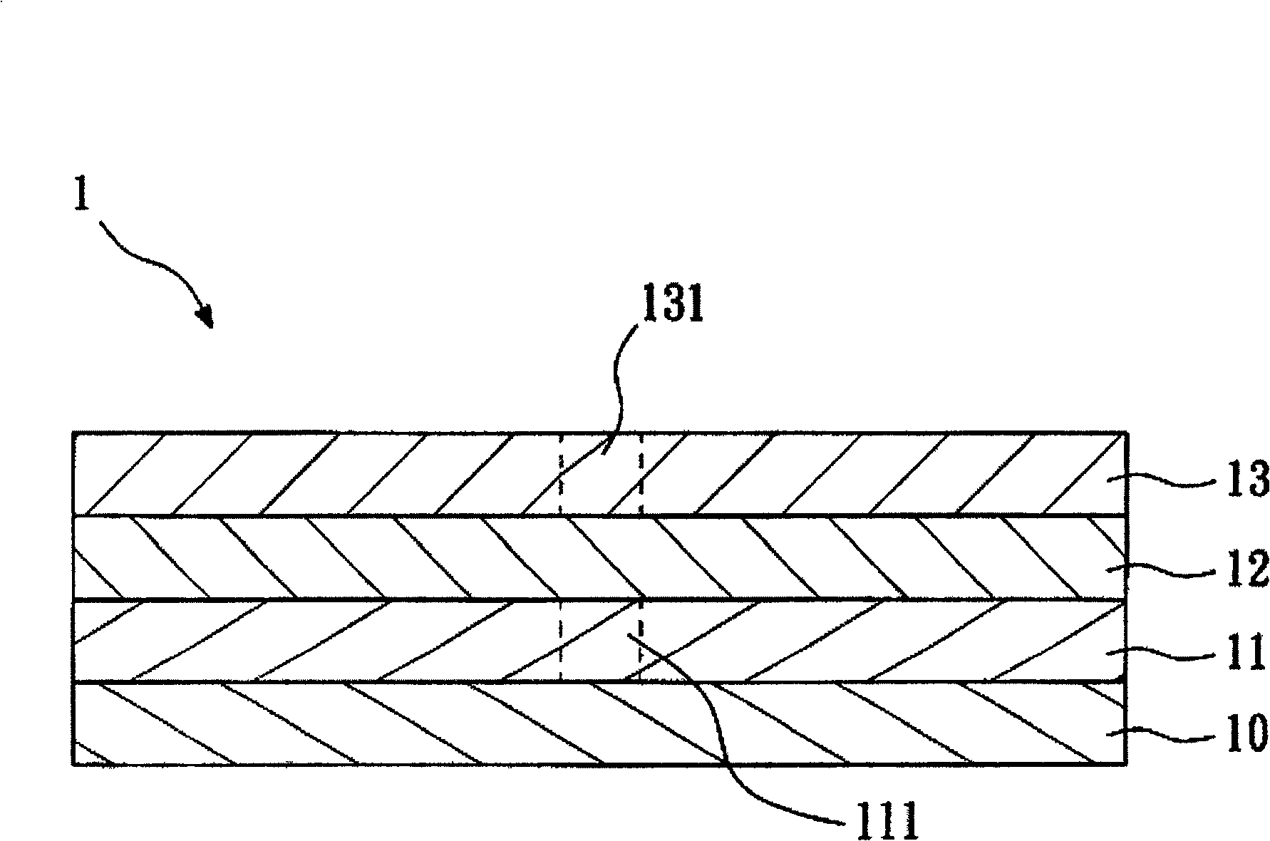
technical field [0001] The invention relates to a method and system for repairing bright spot areas of flat panel displays, in particular to a method and system for repairing bright spot areas of flat panel displays using pulsed lasers. Background technique [0002] refer to figure 1 , which shows a schematic diagram of a conventional flat panel display. The flat panel display 1 has a backlight module 10 , a thin film transistor substrate 11 , a liquid crystal layer 12 and a filter substrate 13 . The thin film transistor substrate 11 is disposed on the backlight module 10 , the liquid crystal layer 12 is disposed on the thin film transistor substrate 11 , and the filter substrate 13 is disposed on the liquid crystal layer 12 . A TFT (not shown) of the TFT substrate 11 is damaged, so that the TFT substrate 11 has a light-transmitting region 111 , and the light-transmitting region 111 cannot block the light generated by the backlight module 10 . The filter substrate 13 has ...

Claims


Application Information

Patent Timeline
Patent Type & Authority Patents(China)
IPC IPC(8): G02F1/13
Inventor 叶昭永
Owner METAL INDS RES & DEV CENT
Learn More