
A kind of preparation method of integrated passive device

A technology for integrating passive devices and bottom metal layers, applied in semiconductor/solid-state device manufacturing, electrical components, circuits, etc., can solve problems such as opening of metal vias, cracking of dielectric layers, and inability to obtain filling effects

Active Publication Date: 2017-09-01
SEMICON MFG INT (SHANGHAI) CORP
View PDF4 Cites 0 Cited by
  • Summary
  • Abstract
  • Description
  • Claims
  • Application Information

AI Technical Summary

Problems solved by technology

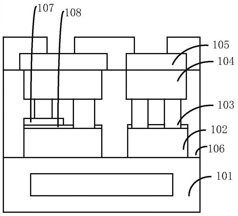
[0006] Due to the increase in the thickness of the metal and dielectric, it is often found that the dielectric layer cracks due to excessive local stress in the chip during the packaging process. From the WAT and XSEM analysis results, it can be known that the cracking phenomenon generally occurs in the bottom metal layer 102 or above the MIM, causing metal vias 103 to open, resulting in chip failure
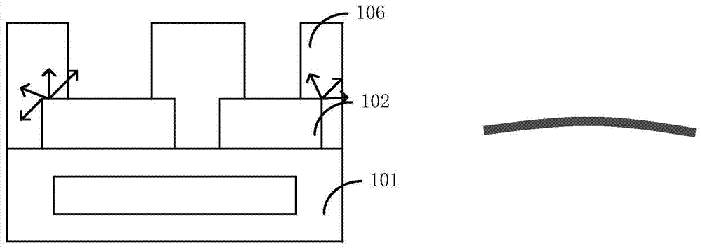
[0007] The reason why the fracture occurs above the bottom metal layer 102 or the MIM during the packaging process is that the current minimum distance between the bottom metal layers 102 is 4um, so the dielectric layer 106 of the bottom metal layer 102 in the current IPD process mainly adopts the HDP method Only by filling can a non-porous dense oxide layer with good step coverage be obtained, and a good filling effect cannot be obtained directly by other CVD methods
However, the disadvantage of HDP compared to other methods is that the HDP oxide layer has a higher stress

Method used


Image

  • A kind of preparation method of integrated passive device
  • A kind of preparation method of integrated passive device
  • A kind of preparation method of integrated passive device

Examples


Embodiment Construction

[0030] In the following description, numerous specific details are given in order to provide a more thorough understanding of the present invention. It will be apparent, however, to one skilled in the art that the present invention may be practiced without one or more of these details. In other examples, some technical features known in the art are not described in order to avoid confusion with the present invention.

[0031] In order to thoroughly understand the present invention, detailed steps will be provided in the following description, so as to illustrate a method for preparing an integrated passive device proposed by the present invention. Obviously, the practice of the invention is not limited to specific details familiar to those skilled in the semiconductor arts. Preferred embodiments of the present invention are described in detail below, however, the present invention may have other embodiments besides these detailed descriptions.

[0032] It should be understoo...


PUM


Abstract

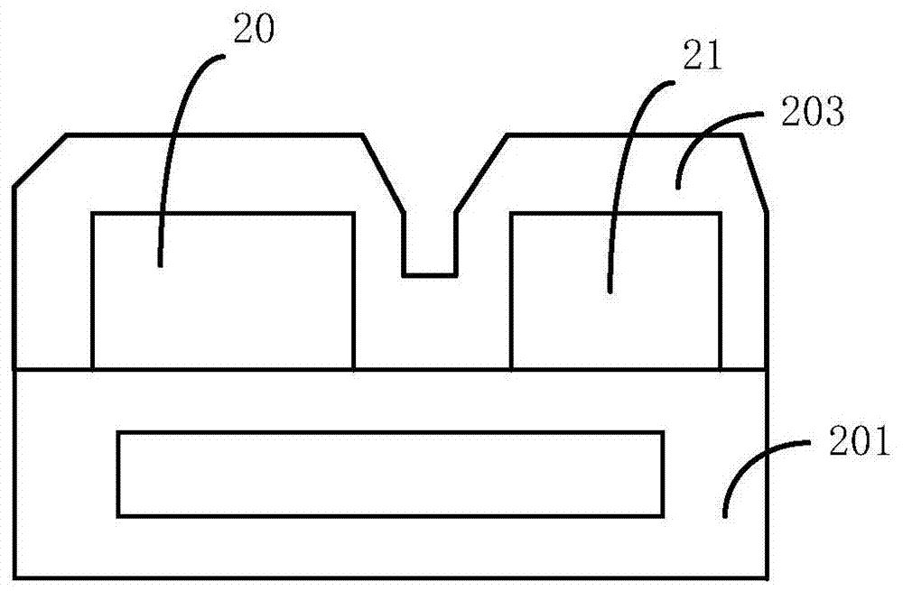
The invention relates to a preparation method of an integrated passive device, comprising: providing a substrate, on which a first bottom metal layer and a second bottom metal layer isolated from each other are formed, and a bottom metal layer is formed between the bottom metal layers There is a gap; deposit a PETEOS layer on the substrate and on the bottom metal layer to fill the gap; deposit a high density plasma oxide layer on the tetraethyl silicate layer; perform a planarization step to the Orthosilicate layer. In the present invention, the PETEOS20K+10KHDP process is selected. Although HDP will bring greater stress after the deposition of the HDP oxide, because in the subsequent CMP process, most of the HDP oxide layer will be ground away. In the end, only the TEOS layer and very little HDP oxide are left, so compared with other conditions, after the via hole is etched, the dielectric layer will not be cracked, which solves the problems existing in the prior art well.

Description

technical field [0001] The invention relates to the field of semiconductors, in particular, the invention relates to a method for preparing an integrated passive device. Background technique [0002] For the increasing demand for high-capacity semiconductor storage devices, the integration density of these semiconductor storage devices has attracted people's attention. In order to increase the integration density of semiconductor storage devices, many different methods have been adopted in the prior art, such as by reducing the wafer size. And / or change the internal structure unit to form multiple memory units on a single wafer. For the method of increasing the integration density by changing the unit structure, attempts have been made to reduce the unit area. [0003] With the continuous development of semiconductor technology, integrated circuits and large-scale integrated circuits are widely used. The components that make up integrated circuits can be passive or active. ...

Claims


Application Information

Patent Timeline
Patent Type & Authority Patents(China)
IPC IPC(8): H01L21/70H01L21/768
Inventor 戚德奎张海芳
Owner SEMICON MFG INT (SHANGHAI) CORP
Learn More