Film transistor array substrates and its producing method, repairing method

A technology of thin film transistors and array substrates, applied in the fields of thin film transistor array substrates and its manufacture and repair, to achieve the effect of convenient and simple repair, without affecting the aperture ratio, and increasing the effect of existing processes

Active Publication Date: 2009-01-21
NANJING CEC PANDA LCD TECH
View PDF7 Cites 0 Cited by
  • Summary
  • Abstract
  • Description
  • Claims
  • Application Information

AI Technical Summary

Problems solved by technology

[0006] Another technical problem to be solved by the present invention is to provide a method for manufacturing a thin-film transistor array substrate capable of repairing disconnection of data lines or gate scanning lines without increasing the existing process and without affecting the aperture ratio.

Method used


Image

  • Film transistor array substrates and its producing method, repairing method
  • Film transistor array substrates and its producing method, repairing method
  • Film transistor array substrates and its producing method, repairing method

Examples


Embodiment 1

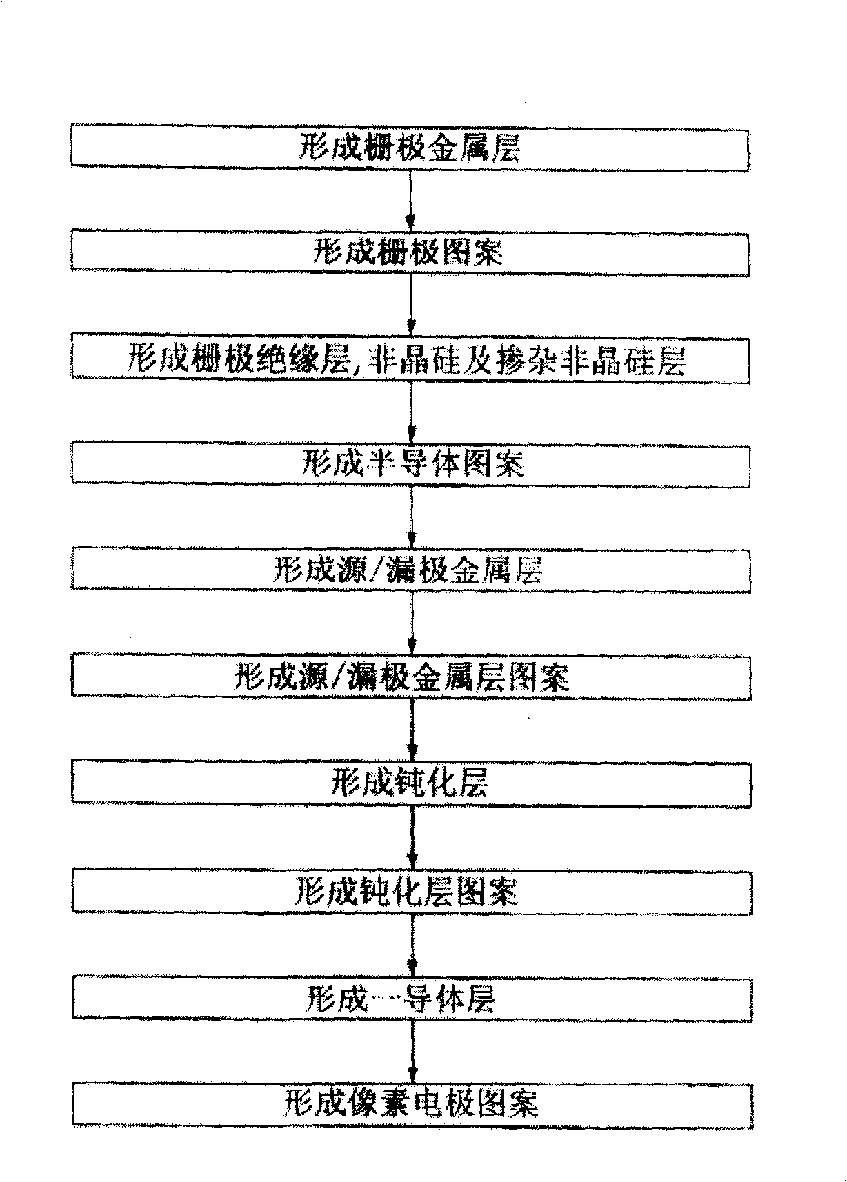
[0029] figure 2 , image 3 is a schematic structural view of a thin film transistor array substrate according to Embodiment 1 of the present invention.

[0030] refer to figure 2 The thin film transistor array substrate includes a plurality of gate scanning lines 10 extending along a first direction; a plurality of data lines 20 extending along a second direction, the gate scanning lines 10 and the data lines 20 intersect to form a pixel area; Thin film transistor 40 and pixel electrode 30, metal pattern 11 is formed on gate scan line 10, thin film transistor 40 is made up of gate 41, source 42 and drain 43, gate 41 is electrically connected with gate scan line 10, drain The electrode 43 is electrically connected to the data line 20, the source electrode 42 is connected to the pixel electrode 30 through the contact hole 41, the gate electrode 41 and the gate scanning line 10 are formed on the first metal layer (M1), the source electrode 42, the drain electrode 43, The dat...

Embodiment 2

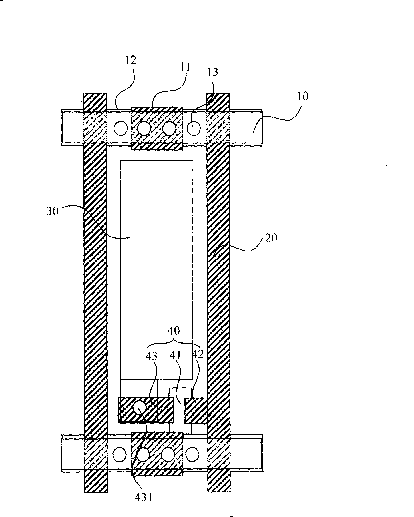
[0039] Figure 4 is a schematic structural view of a thin film transistor array substrate according to Embodiment 2 of the present invention.

[0040] refer to Figure 4 Different from the structure of the TFT array substrate provided in Embodiment 1, metal patterns 21 are formed under the data lines 20 in this embodiment, and the metal patterns 21 are formed on the same layer as the gate scanning lines 10 . The material of the metal pattern 21 is the same as that of the gate scan line 10 . In the process of manufacturing the array substrate, when patterning the first metal layer, the metal pattern 21 corresponding to the data line 20 is reserved, and the metal pattern 21 is compatible with other metal patterns of the same layer such as the gate 41 and the gate scanning line 10. separated from each other.

[0041] When an open circuit occurs on the data line 20, laser welding can be performed on both sides of the broken line from the back of the array substrate (outside the...


PUM


Abstract

The invention discloses a thin film transistor array substrate and manufacturing and repairing methods of the thin film transistor array substrate which comprises a plurality of grid scanning lines extending along a first direction and a plurality of data lines extending along a second direction. The grid scanning lines and the data lines intersect with each other and form a pixel region, in which a thin film transistor and a pixel electrode are arranged. Metal pattern formed above the grid scanning lines or below the data lines are separated from the data lines metal layer pattern and the grid scanning lines metal layer pattern. The invention can repair the broken-circuit of the data lines and the grid scanning lines in the pixel section without additional fabrication procedure of the existing array substrate and with simple and convenient repairing.

Description

technical field [0001] The invention relates to an array substrate and its manufacturing method and repairing method, in particular to a thin film transistor array substrate for liquid crystal display capable of repairing line defects, its manufacturing method and its repairing method. Background technique [0002] Thin film transistor liquid crystal display (TFT-LCD) panels use thin film transistors (TFT) to control the orientation of liquid crystal molecules to control the intensity of light transmission to display images. A complete TFTLCD panel usually includes a backlight module, a polarizer, a TFT array substrate, a CF (color filter) substrate, a liquid crystal molecular layer sandwiched between the upper and lower substrates, and a driving circuit. The display area on the TFT array substrate includes a plurality of sub-pixel areas, and each sub-pixel area is generally a rectangular or other shaped area formed by the intersection of two gate scanning lines and two data...

Claims


Application Information

Patent Timeline
Patent Type & Authority Patents(China)
IPC IPC(8): H01L27/12H01L23/525H01L21/84H01L21/768G02F1/1362G02F1/1343G02F1/1333
Inventor 田广彦
Owner NANJING CEC PANDA LCD TECH
Why Eureka
Try Eureka