Charging circuit and/or discharge circuit and carrier detection circuit using them

A technology of charging circuit and discharging circuit, which is applied in the field of carrier detection circuit, can solve the difficult problems of separation and unacceptability of the noise of the fluorescent lamp starter and the carrier

Inactive Publication Date: 2009-03-25
SHARP KK
View PDF1 Cites 0 Cited by
  • Summary
  • Abstract
  • Description
  • Claims
  • Application Information

AI Technical Summary

Problems solved by technology

In consideration of the Early effect, in order to form an acceptable duty within the specification range, the duty ratio is set high, which makes it difficult to separate the noise and the carrier wave of the fluorescent lamp starter, resulting in unacceptable and erroneous operation. The main reason

Method used


Image

  • Charging circuit and/or discharge circuit and carrier detection circuit using them
  • Charging circuit and/or discharge circuit and carrier detection circuit using them
  • Charging circuit and/or discharge circuit and carrier detection circuit using them

Examples


Embodiment Construction

[0055] Below, according to figure 1 The first embodiment of the present invention will be described.

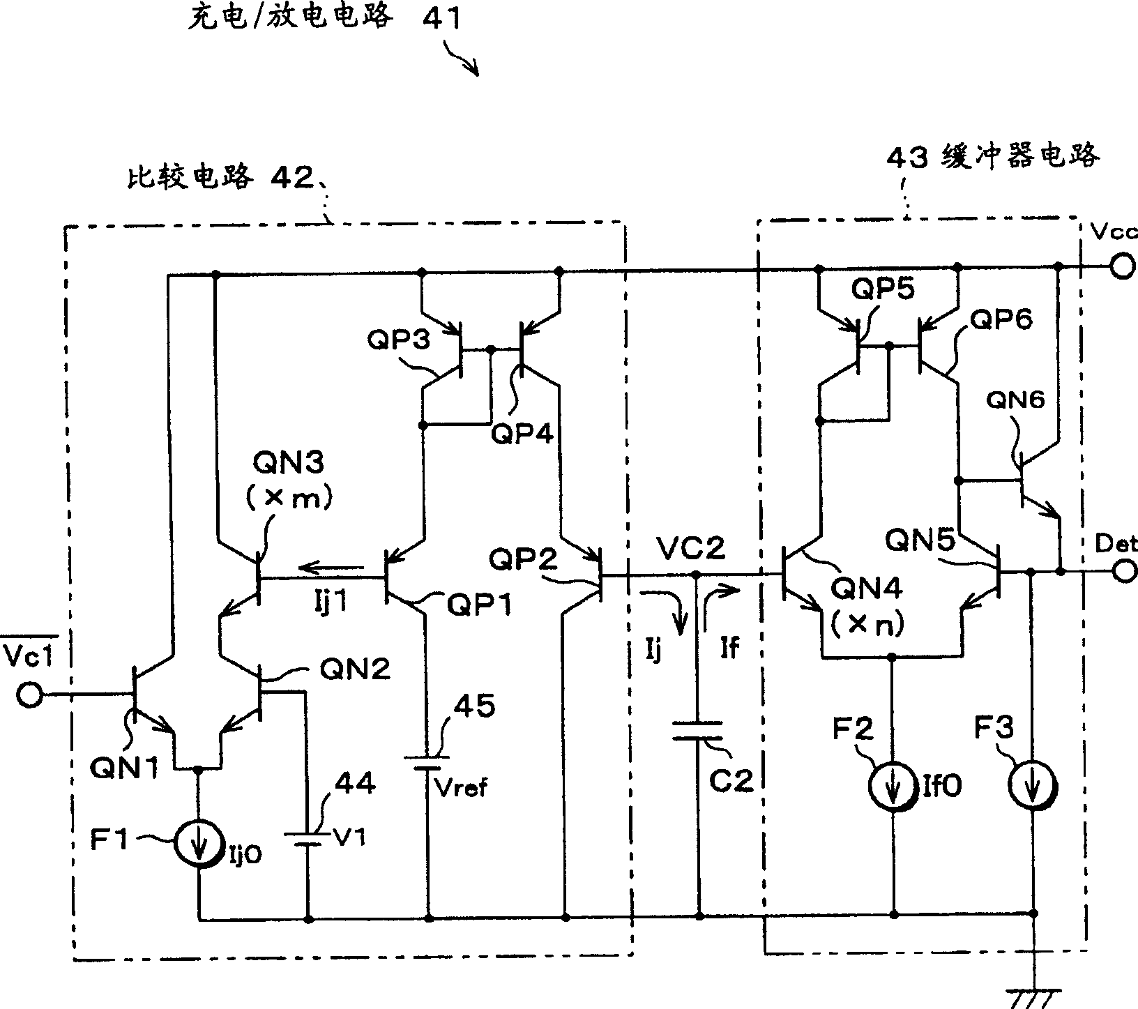
[0056] figure 1 It is a circuit diagram of the charging and discharging circuit 41 of the first embodiment of the present invention. The charging and discharging circuit 41 is composed of a capacitor C2, a comparator circuit 42 that outputs a small current, and a buffer circuit 43 that inputs a small current. In this configuration, it is indicated that the output Vc1 of the wave detector 21 is not directly input to the comparison circuit 42, but its inverted output Vc1 is input as shown in FIG. 6(c). -1 case.

[0057] In the comparison circuit 42, the inverted output Vc1 is supplied to the bases of the transistors QN1, QN2 forming a differential pair, respectively. -1 and the reference voltage V1 from the reference voltage source 44 . The emitters of the transistors QN1 and QN2 are grounded through the constant current source F1, the collector of the transistor QN1 is ...


PUM


Abstract

A charge / discharge circuit creates a carrier detection level based on a received signal in a carrier detector circuit for detecting the presence or absence of a carrier in such applications as a receiver for an IR remote controller. The charge / discharge circuit operates to amplify a current, that is produced in N-type transistors QN1, QN2, QN3 and a reference current source, in a P-type transistor QP1. The amplified current is mirrored by a current mirror circuit to be supplied as an emitter current of a P-type transistor QP2. The charge / discharge circuit charges a capacitor with a small current, i.e., a base current of the P-type transistor QP2. The charge / discharge circuit includes a bias voltage source which produces such a bias voltage that the emitter-collector voltage of the P-type transistor QP1 becomes substantially equal to the emitter-collector voltage of the P-type transistor QP2. As a result, it is possible to limit an error of a charge current charged into the capacitor, which is caused by the emitter-collector voltage dependent change of the collector current and thus the base current, known as the Early effect.

Description

technical field [0001] The present invention relates to a charging and discharging circuit for charging or discharging at least one of capacitors with a fixed current, and a carrier detection circuit using the circuit, which is used for so-called infrared remote control receivers and resolution of signals including carrier waves. Tuner, etc., to form the carrier detection level. Background technique [0002] The infrared remote control receiver is developing toward miniaturization, and can be composed of two chips in which an external photodiode is connected to an IC chip. Therefore, a capacitor that is charged / discharged with or without carrier detection and whose output voltage is at the carrier detection level is required to maintain a small charge and discharge current with high precision as a micro capacitor that can be incorporated in the IC chip. [0003] FIG. 5 is a block diagram showing an example of the configuration of the infrared remote control receiver 1, and ...

Claims


Application Information

Patent Timeline
Patent Type & Authority Patents(China)
IPC IPC(8): H04B1/10H03D1/10H03K17/78H01M10/46
CPCH04B10/69H04L27/06H03D1/10Y02E60/12H04L27/066H04B1/10
Inventor 井上高广横川成一西野毅
Owner SHARP KK
Why Eureka
Try Eureka