

Dual bar and dual stress channel-changing full consumption SOI MOSFETs part structure
A device structure and double-strain technology, applied in the field of microelectronics and solid-state electronics, can solve the problems of subthreshold slope increase and process incompatibility, etc., to eliminate parasitic conductive channels, facilitate integration, and suppress short channels Tao effect
- Summary
- Abstract
- Description
- Claims
- Application Information
AI Technical Summary
Problems solved by technology
Method used
Image

Examples
Embodiment Construction
[0014] The present invention will be described in detail below in conjunction with the accompanying drawings and specific embodiments.
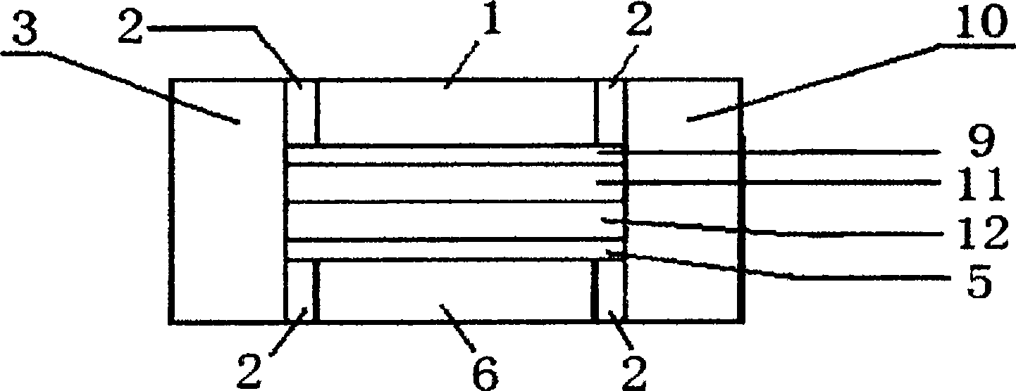
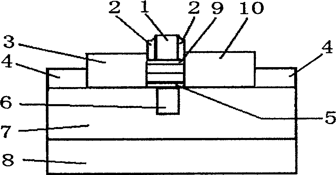
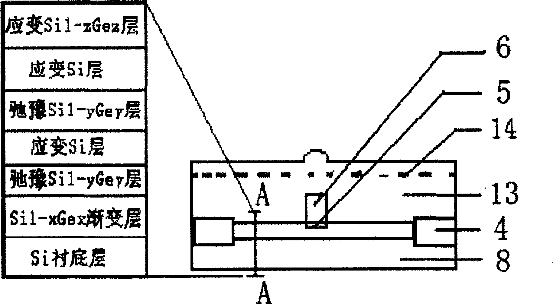
[0015] Such as figure 1 As shown, it is a schematic structural diagram of the present invention, and both sides of the top gate 1 are provided with Si 3 N 4 Side wall 2, Si 3 N 4 A source region 3 is arranged on one side of the side wall 2, and an STI shallow trench isolation region 4 is arranged on the outside of the source region 3, and the Si 3 N 4 The other side of the side wall 2 is provided with a drain region 10, and the outside of the drain region 10 is also provided with an STI shallow trench isolation region 4, and a top gate oxide layer 9 is placed under the top gate 1, and the device channel is formed under the top gate oxide layer 9. The channel area is divided into two layers, the strained Si layer 11 and the strained SiGe layer 12, the upper layer is the strained Si layer 11, the strained SiGe layer 12 is placed under the ...
PUM
 Abstract
Description
Claims
Application Information