
Semiconductor device manufacturing method and substrate treating apparatus

A technology of substrate processing device and manufacturing method, which is applied in the direction of semiconductor/solid-state device manufacturing, electrical components, circuits, etc., and can solve the problem of polluting the surface of the wafer

Active Publication Date: 2009-07-29
KOKUSA ELECTRIC CO LTD
View PDF5 Cites 0 Cited by
  • Summary
  • Abstract
  • Description
  • Claims
  • Application Information

AI Technical Summary

Problems solved by technology

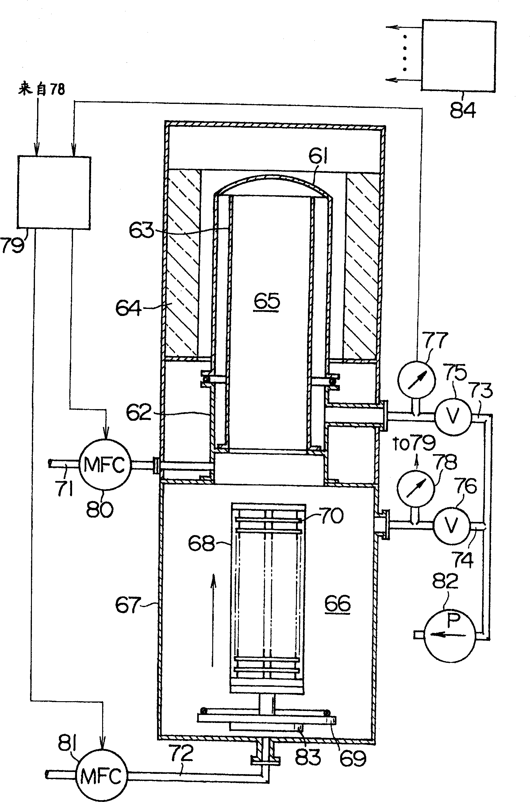
[0007] However, in this CVD apparatus with a pre-chamber, the drive shaft, the boat rotating mechanism, and the wiring for carrying the wafer and the boat into the reaction furnace are placed in the pre-chamber, so it may be damaged by vacuum suction. When organic matter and other pollutants contaminate the wafer surface

Method used


Image

  • Semiconductor device manufacturing method and substrate treating apparatus
  • Semiconductor device manufacturing method and substrate treating apparatus
  • Semiconductor device manufacturing method and substrate treating apparatus

Examples


Embodiment 1

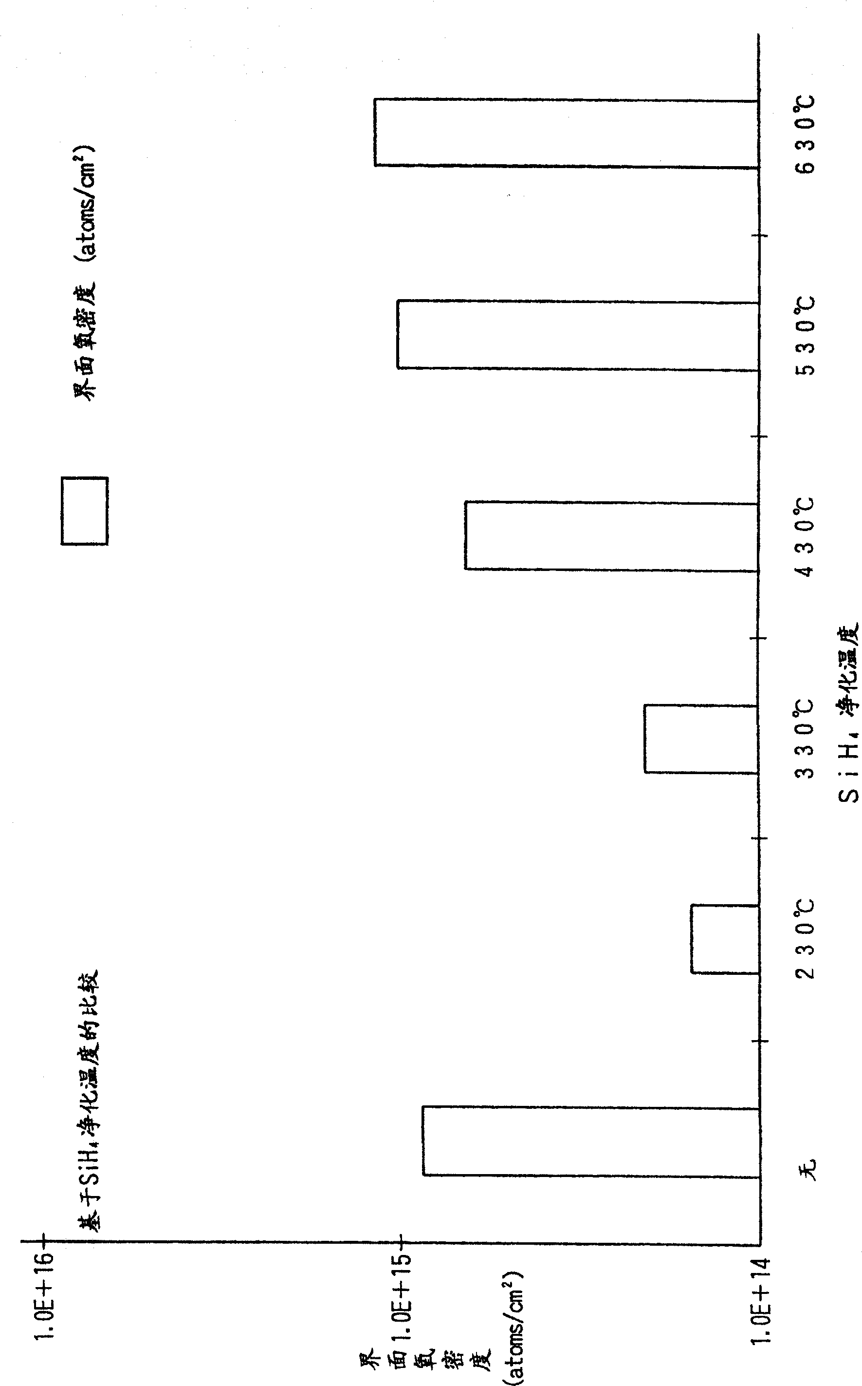
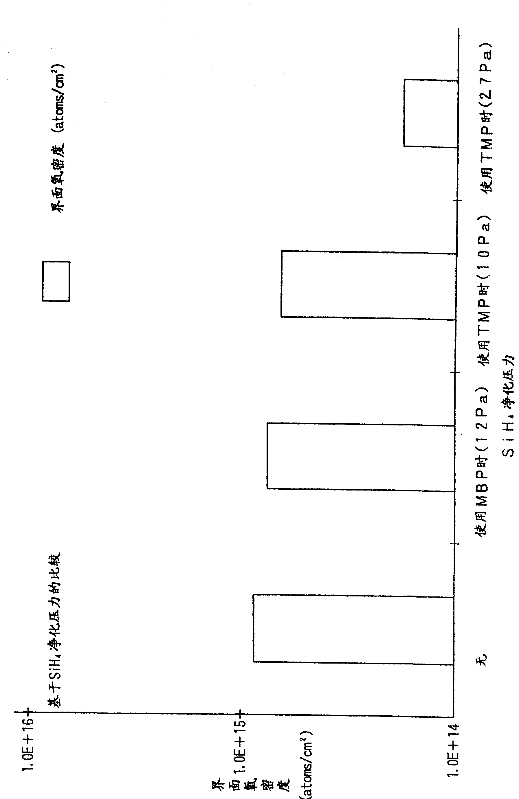
[0176] Next, as a first example, in order to prove SiH 4 The temperature dependence and pressure dependence of the surface oxygen density (concentration) during purification will be described by experiments.

[0177] An example of a semiconductor device requiring a low oxygen density interface is an electrode portion drawn from a source and a drain of a DRAM (Dynamic Random Access Memory). This interface characteristic is called contact resistance, and the smaller the amount of natural oxide film in this part, the lower the contact resistance and improve the electrical characteristics.

[0178] As the evaluation test of this example, aiming at electrical characteristics, D-polySi film (phosphorus-doped polysilicon film) and D-polySi film (phosphorus-doped polysilicon film) were measured by SIMS (Secondary Ionization Mass Spectrometer) interface properties between them.

[0179] In addition, as the evaluation device, the device of the above-mentioned embodiment, that is, a fi...

Embodiment 2

[0204] Next, as a second example, in order to prove SiH 4 The temperature dependence of the purified contact resistance for experiments is described.

[0205] In the second embodiment, based on the SIMS evaluation results of the first embodiment, the interface contact resistance evaluation is carried out using actual equipment.

[0206] Due to the SIMS results according to the first example, SiH at low temperature and high vacuum 4 Purification is effective, so the evaluation was carried out by using TMP with the pressure fixed at 10 Pa, and at two temperatures, 330°C and 430°C, which are lower than the film formation temperature (530°C).

[0207] Figure 4 Indicates the interfacial contact resistance for SiH 4 Dependence of purification temperature.

[0208] The horizontal axis represents SiH 4 Purification temperature (°C), vertical axis represents interface contact resistance (Ω / piece).

[0209] As mentioned above, changing the SiH 4 The purification temperature was ...

Embodiment 3

[0213] Next, as a third example, in order to prove SiH 4 Purified interfacial oxygen density vs. wafer entering furnace to entering SiH 4 The time dependence of the completion of the purification step is illustrated by the experiments performed.

[0214] Figure 5 Indicates the interface oxygen density vs. from the end of the wafer into the furnace to SiH 4 Dependence of time for completion of the purification step (SIMS results).

[0215] The horizontal axis represents the time from the end of the wafer into the furnace to the SiH 4 The time for the completion of the purification step (minutes), the vertical axis represents the interface oxygen density (atoms / cm 2 ).

[0216] Such as Figure 5 As shown, will be from furnace to SiH 4 The time to complete the purification step was changed to 50 minutes and 15 minutes for evaluation.

[0217] according to Figure 5 It can be seen that from the furnace to the SiH 4 When the time to complete the purge step is short, the ...


PUM


Abstract

The present invention relates to a semiconductor device manufacturing method. A high quality interface is formed at a low oxygen / carbon density between a substrate and a thin film while preventing heat damage on the substrate and increase of thermal budget. A semiconductor device manufacturing method has a step of carrying a wafer into a reacting furnace, a step of performing pretreatment to the wafer in the reacting furnace, a step of performing main treatment to the wafer to which the pretreatment has been performed in the reacting furnace, and a step of carrying out the wafer from the reacting furnace after the main treatment. During a period between the completion of pretreatment and start of main treatment, hydrogen gas is constantly and continuously supplied to the reacting furnace at least at the time of vacuumizing the reacting furnace.

Description

technical field [0001] The present invention relates to a manufacturing method of a semiconductor device (semiconductor device) and a substrate processing device, for example, to a manufacturing method of a semiconductor integrated circuit device (hereinafter referred to as IC) which is effective in forming a semiconductor device including a semiconductor element. The process of forming a thin film on a semiconductor wafer (wafer) (hereinafter referred to as a wafer) of an integrated circuit, especially relates to the technology of forming a high-quality interface between a silicon wafer and a thin film. Background technique [0002] In the IC manufacturing method, a thin film is formed on a wafer by a reduced-pressure CVD method (chemical vapor phase growth method). [0003] In recent years, in order to solve the problem of semiconductor deterioration caused by thickening of the natural oxide film or adhesion of impurities when the wafer is introduced into the reaction furn...

Claims


Application Information

Patent Timeline
Patent Type & Authority Patents(China)
IPC IPC(8): H01L21/205
Inventor 尾崎贵志笠原修野田孝晓前田喜世彦森谷敦坂本农
Owner KOKUSA ELECTRIC CO LTD
Learn More