Semiconductor device having IGBT and diode

A diode and semiconductor technology, applied in the field of semiconductor devices, can solve problems such as smaller breakdown energy, small surge withstand voltage, and easy function of parasitic NPN transistors

Active Publication Date: 2007-07-18
DENSO CORP
View PDF2 Cites 13 Cited by
  • Summary
  • Abstract
  • Description
  • Claims
  • Application Information

AI Technical Summary

Problems solved by technology

In this case, when a high voltage surge is applied to the device 91, and an avalanche current flows into the P conductivity type region 2w, the parasitic NPN transistor easily functions so that the device 91 is damaged by the high voltage surge
Therefore, although the recovery performance of the diode unit 91d is improved, the breakdown energy becomes small so that the device 91 has a small surge withstand voltage

Method used


Image

  • Semiconductor device having IGBT and diode
  • Semiconductor device having IGBT and diode
  • Semiconductor device having IGBT and diode

Examples


no. 1 example

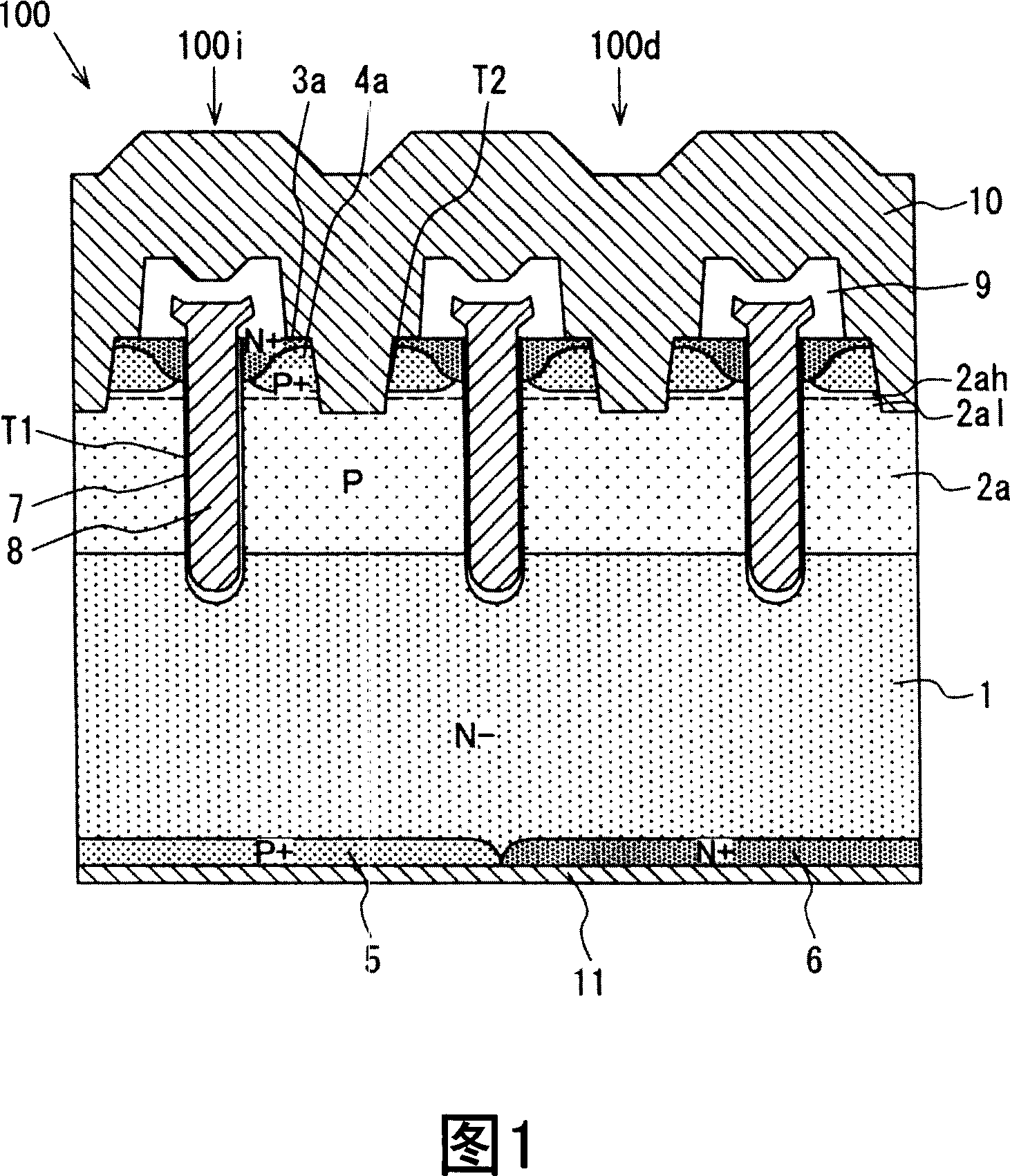
[0037] FIG. 1 shows a semiconductor device 100 according to a preferred embodiment. The device 100 includes an IGBT cell 100i and a diode cell 100d formed in the same substrate 1 . Device 100 includes a N - Conductive type semiconductor substrate 1 . The P conductive type layer 2a is formed on the main surface of the substrate 1, and the impurity concentration of the P conductive type region 2a gradually decreases from the surface portion to the inner portion. N on the main surface side with high impurity concentration + Conductivity type region 3a (ie, main N region) and P on the main surface side with high impurity concentration + The conductivity type region 4a (ie, the main P region) is formed on the surface portion of the P conductivity type region 2a. The main P region 4a is formed by the diffusion method so that the main P region 4a does not reach the PN junction between the P conductive type region 2a and the main N region 3a. The main P region 4a is provided in t...


PUM


Abstract

A semiconductor device includes: a substrate having a first side and a second side; an IGBT; and a diode. The substrate includes a first layer, a second layer on the first layer, a first side N region on the second layer, second side N and P regions on the second side of the first layer, a first electrode in a first trench for a gate electrode, a second electrode on the first side N region and in a second trench for an emitter electrode and an anode electrode, and a third electrode on the second side N and P regions for a collector electrode and a cathode. The first trench penetrates the first side N region and the second layer, and reaches the first layer. The second trench penetrates the first side N region, and reaches the second layer.

Description

technical field [0001] The present invention relates to a semiconductor device having an IGBT and a diode. Background technique [0002] Inverter circuits for driving loads such as electric motors are converters for switching between DC and AC. Thus, the converter converts the DC voltage to an AC voltage so that the inverter circuit powers the load. Inverter circuits for driving induction type motors include IGBTs (ie, insulated gate bipolar transistors) and FWDs (ie, freewheeling diodes). IGBTs provide switching devices. When the IGBT is turned off, the FWD bypasses the current flowing through the motor, so that the FWD controls the current flowing through the motor unchanged to counteract the switching operation of the IGBT. Specifically, the IGBT is electrically coupled between the DC power source and the motor so that a predetermined voltage is applied to the motor. When the IGBT is turned off, the current flowing through the motor flows back to the DC source through...

Claims


Application Information

Patent Timeline
IPC IPC(8): H01L27/06
Inventor 都筑幸夫户仓规仁
Owner DENSO CORP
Why Eureka
Try Eureka