Semiconductor device having IGBT and diode

a technology of igbt and diode, which is applied in the direction of diodes, semiconductor devices, electrical apparatus, etc., can solve the problems of difficult improvement of diode performance, low recovery performance, and deterioration of igbt cell performance, so as to reduce recovery loss in the device, the surge resistance is sufficient, and the igbt performance is sufficien

Active Publication Date: 2007-07-26
DENSO CORP
View PDF19 Cites 47 Cited by
  • Summary
  • Abstract
  • Description
  • Claims
  • Application Information

AI Technical Summary

Benefits of technology

[0022]In the above device, the second layer provides a channel of the IGBT and a P conductive portion of the diode. The device has sufficient IGBT performance and sufficient surge withstand voltage. Further, the second layer connecting to the anode of the diode has the impurity concentration, which is reduced from the surface portion to the inside of the second layer. Thus, an introduced hole concentration is reduced in case of forward operation, so that a recovery current in case of reverse recovery process becomes small. Thus, the recovery loss in the device is reduced so that the recovery characteristics are improved.
[0024]In the above device, the second layer provides a channel of the IGBT and an N conductive portion of the diode. The device has sufficient IGBT performance and sufficient surge withstand voltage. Further, the second layer connecting to the cathode of the diode has the impurity concentration, which is reduced from the surface portion to the inside of the second layer. Thus, an introduced hole concentration is reduced in case of forward operation, so that a recovery current in case of reverse recovery process becomes small. Thus, the recovery loss in the device is reduced so that the recovery characteristics are improved.

Problems solved by technology

Accordingly, recovery performance becomes low.
However, since the diode cell 90d is formed together with the IGBT cell 90i, structure change such as the above optimization for improving the diode performance may deteriorate the performance of the IGBT cell 90i.
Thus, it is difficult to improve the diode performance.

Method used


Image

  • Semiconductor device having IGBT and diode
  • Semiconductor device having IGBT and diode
  • Semiconductor device having IGBT and diode

Examples


first embodiment

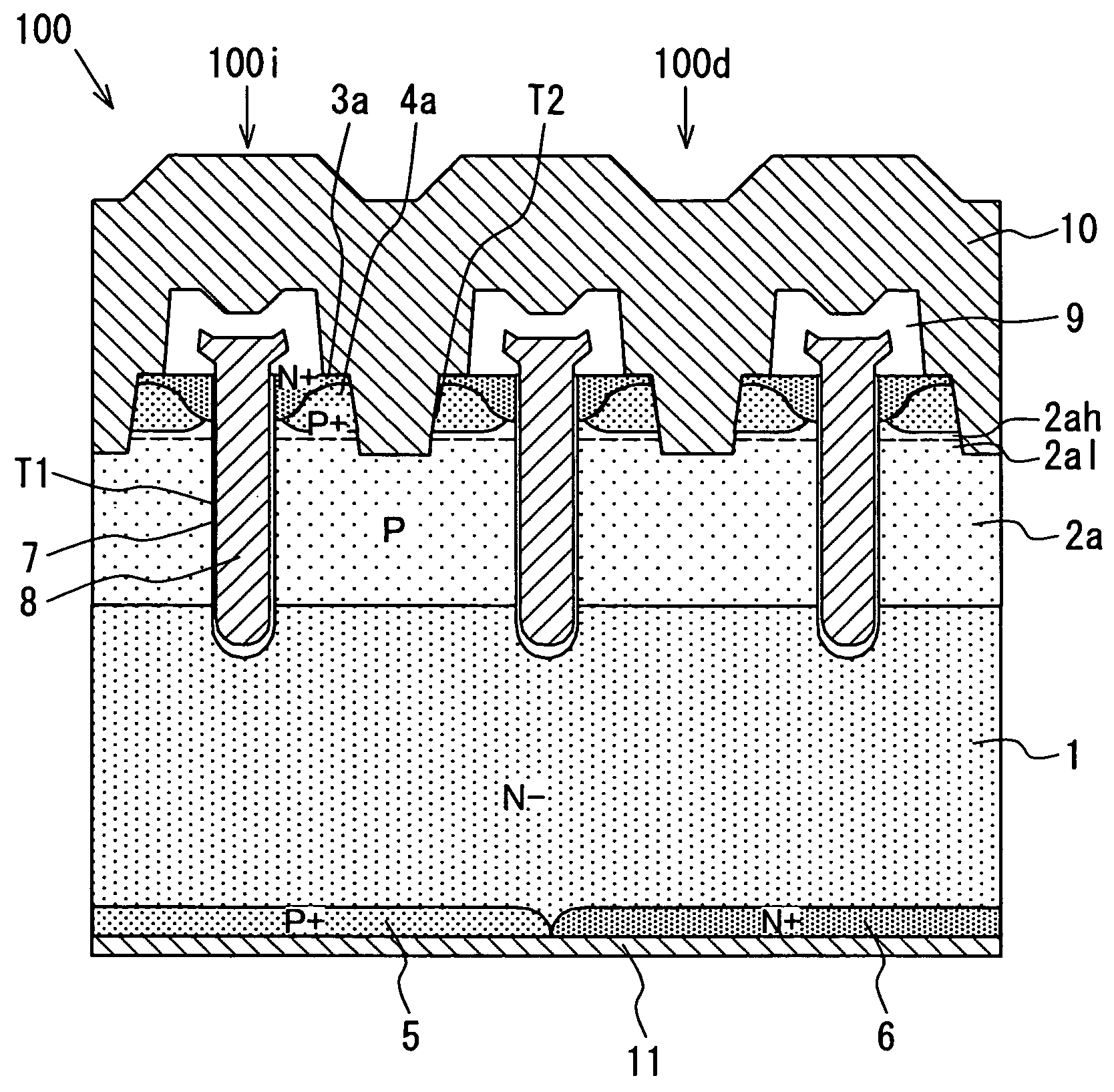
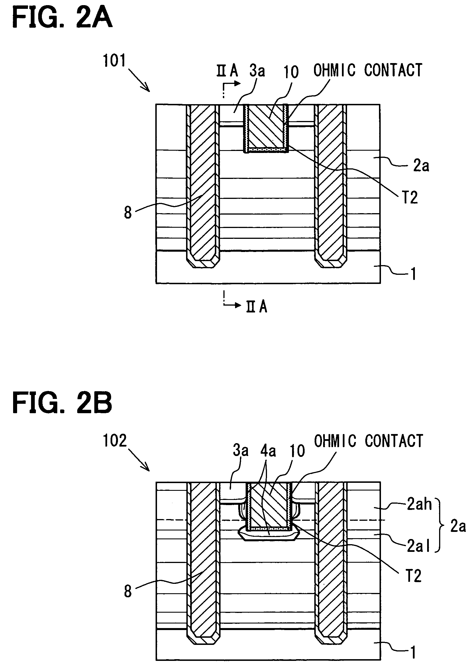
[0037]FIG. 1 shows a semiconductor device 100 according to a preferred embodiment. The device 100 includes an IGBT cell 100i and a diode cell 100d, which are formed in a same semiconductor substrate 1. The device 100 includes a N− conductive type semiconductor substrate 1 having a principal surface and a backside surface. A P conductive type layer 2a is formed on the principal surface of the substrate 1, and an impurity concentration of the P conductive type region 2a is gradually reduced from a surface portion to an inner portion. A principal surface side N+ conductive type region 3a (i.e., a principal N region) having a high impurity concentration and a principal surface side P+ conductive type region 4a (i.e., principal P region) having a high impurity concentration are formed on the surface portion of the P conductive type region 2a. The principal P region 4a is formed by a diffusion method such that the principal P region 4a does not reach the PN junction between the P conducti...


PUM


Abstract

A semiconductor device includes: a substrate having a first side and a second side; an IGBT; and a diode. The substrate includes a first layer, a second layer on the first layer, a first side N region on the second layer, second side N and P regions on the second side of the first layer, a first electrode in a first trench for a gate electrode, a second electrode on the first side N region and in a second trench for an emitter electrode and an anode electrode, and a third electrode on the second side N and P regions for a collector electrode and a cathode. The first trench penetrates the first side N region and the second layer, and reaches the first layer. The second trench penetrates the first side N region, and reaches the second layer.

Description

CROSS REFERENCE TO RELATED APPLICATIONS[0001]This application is based on Japanese Patent Applications No. 2006-2874 filed on Jan. 10, 2006, and No. 2006-322900 filed on Nov. 30, 2006, the disclosures of which are incorporated herein by reference.FIELD OF THE INVENTION[0002]The present invention relates to a semiconductor device having an IGBT and a diode.BACKGROUND OF THE INVENTION[0003]An inverter circuit for driving a load such as a motor is a converter for switching a direct current and an alternating current. Thus, the converter converts a direct voltage to an alternating voltage so that the inverter circuit supplies electricity to the load. The inverter circuit for driving an inductive type motor includes an IGBT (i.e., insulated gate bipolar transistor) and a FWD (i.e., free wheel diode). The IGBT provide s switching device. The FWD bypasses the current flowing through the motor when the IGBT turns off so that the FWD controls the current flowing through the motor to be const...

Claims


Application Information

Patent Timeline
Patent Type & Authority Applications(United States)
IPC IPC(8): H01L27/082
CPCH01L27/0664H01L29/861H01L29/7397H01L29/0834
Inventor TSUZUKI, YUKIOTOKURA, NORIHITO
Owner DENSO CORP
Why Eureka
Try Eureka