Method for manufacturing an optical film, apparatus for manufacturing the same, optical film, polarizing plate and image display device

An optical film and film technology, applied in the device, optics, polarizing element and other directions of coating liquid on the surface, can solve the problems of not getting film, uneven visual color, quality problems, etc.

Active Publication Date: 2007-07-18
FUJIFILM CORP
View PDF35 Cites 17 Cited by
  • Summary
  • Abstract
  • Description
  • Claims
  • Application Information

AI Technical Summary

Problems solved by technology

However, there is a limit to the concentration of oxygen that can be replaced by nitrogen to effectively produce an anti-reflection film on a web, so that a film with a desired hardness cannot be obtained.
[0008] Patent documents JP-A-11-268240, JP-A-60-90762, JP-A-59-112870, JP-A-4-301456, JP-A-3-67967 and JP-A-2003-300215 are disclosed A special means for carrying out nitrogen replacement has been proposed, however, this means poses a problem in that a large amount of nitrogen is required to sufficiently reduce the concentration of oxygen to cure a thin film such as a low-refractive layer, thus resulting in an increase in manufacturing cost
[0012] When the anti-reflection layer is used in image display devices, these coating thickness irregularities of the anti-reflection layer can cause visual color unevenness to be perceived, causing serious quality problems

Method used


Image

  • Method for manufacturing an optical film, apparatus for manufacturing the same, optical film, polarizing plate and image display device
  • Method for manufacturing an optical film, apparatus for manufacturing the same, optical film, polarizing plate and image display device
  • Method for manufacturing an optical film, apparatus for manufacturing the same, optical film, polarizing plate and image display device

Examples


Embodiment Construction

[0112] Best Mode for Carrying Out the Invention

[0113] Hereinafter, the present invention will be described in detail. In this specification, "(numerical value 1) to (numerical value 2)" means "not less than (numerical value 1) but not more than (numerical value 2)" when numerical values ​​represent physical property values, characteristic values, etc.

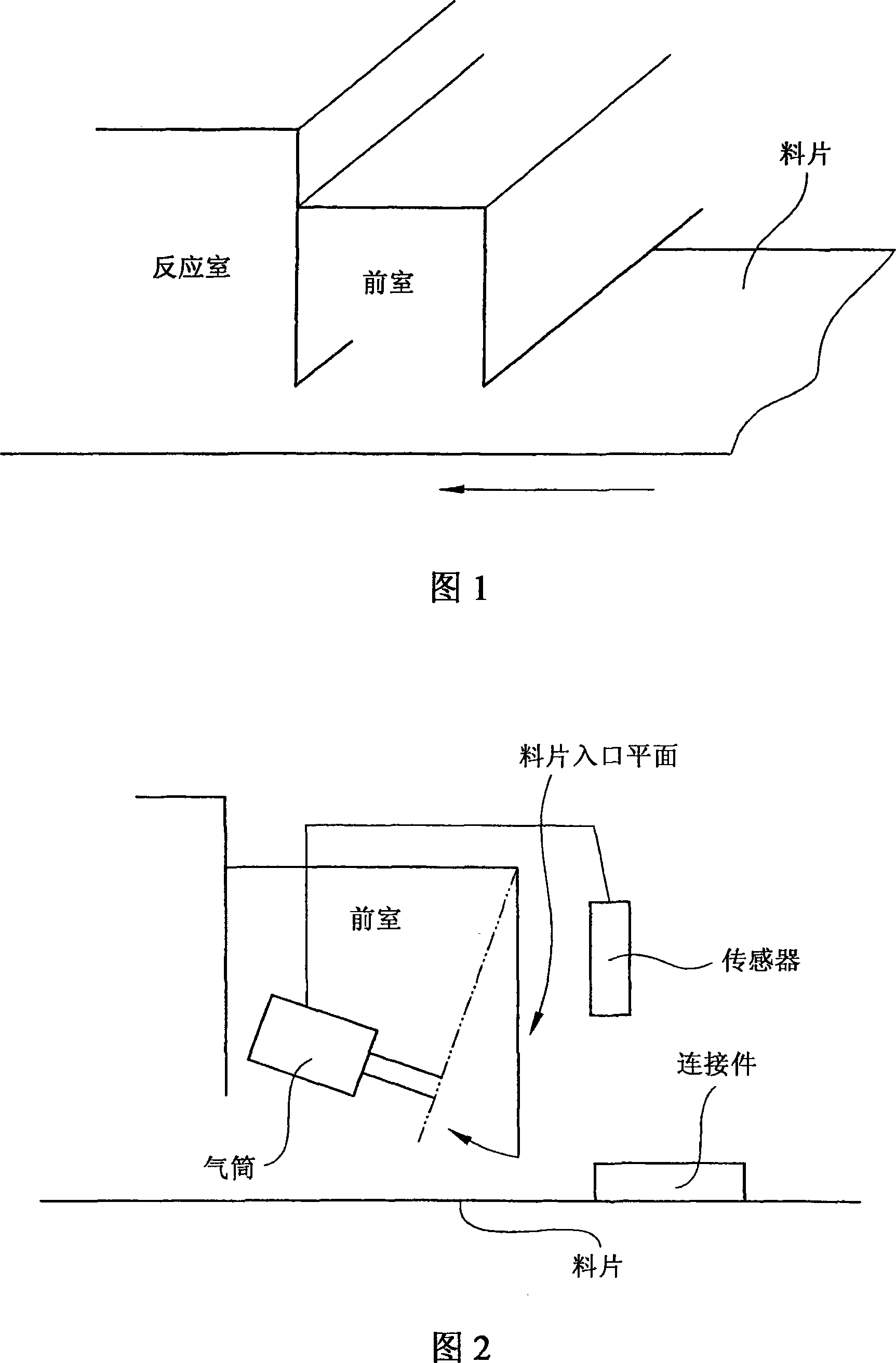
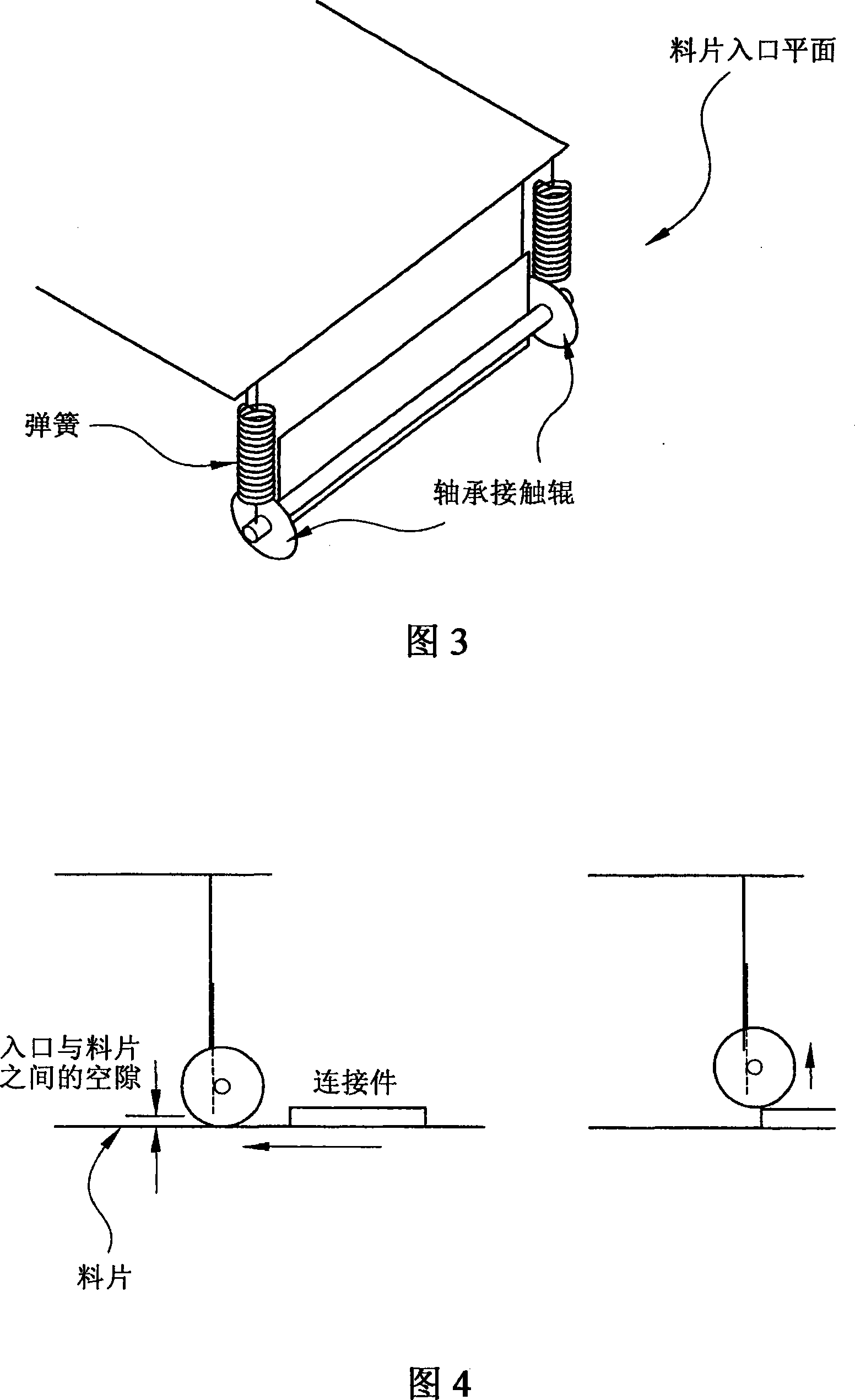
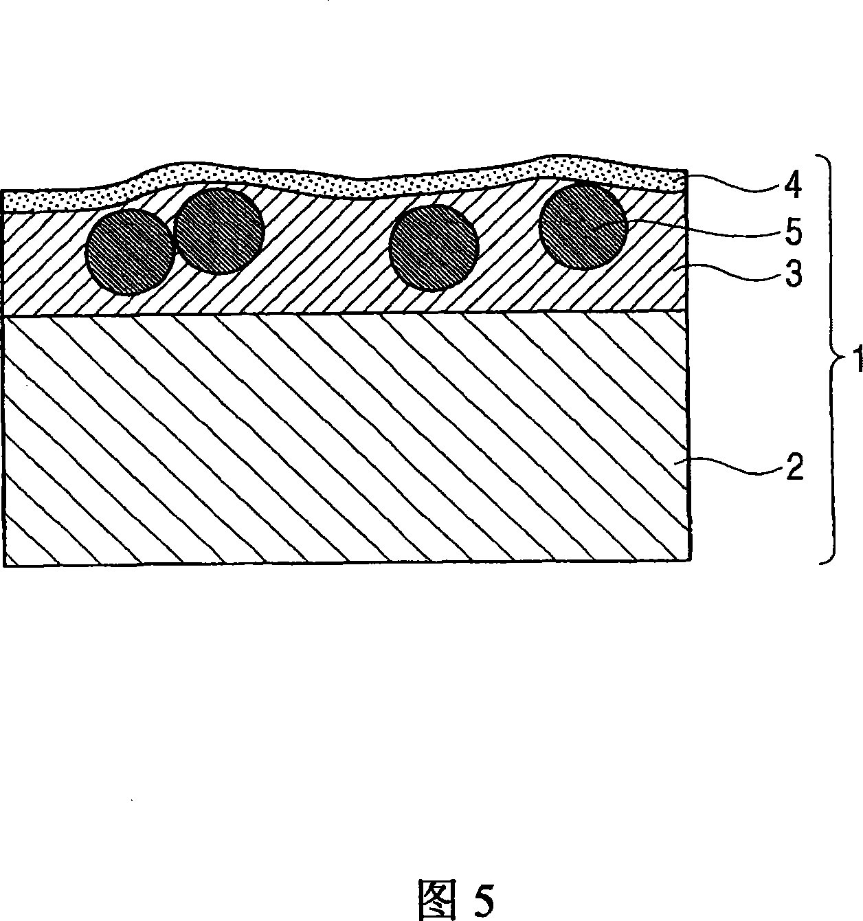
[0114] [Layered structure of optical film]

[0115]The optical film of the present invention has at least one functional layer on a transparent substrate (hereinafter sometimes referred to as a substrate film). In this case, the functional layer includes, for example, an antistatic layer, a hard coat layer (cured resin layer), an antireflection layer, an antiglare layer, an optional compensation layer, an alignment layer, and a liquid crystal layer. Wherein, when necessary, the antireflection film of the present invention has a hard coat layer (described below) on a transparent substrate, and also has an antireflection lay...


PUM

PropertyMeasurementUnit
lengthaaaaaaaaaa
thicknessaaaaaaaaaa
thicknessaaaaaaaaaa

Abstract

A method for manufacturing an optical film comprising a transparent substrate and at least one functional layer on or above the transparent substrate, wherein said at least one functional layer to be laminated on the transparent substrate is formed by a layer-forming method comprising the following steps (1) and (2): (1) step of applying a coated layer on the transparent substrate, and (2) step of curing the coated layer by irradiating ionizing radiation in an oxygen environment in which the oxygen concentration is lower than an atmospheric oxygen concentration.

Description

technical field [0001] The present invention relates to a method for manufacturing an optical film having excellent abrasion resistance / scratch resistance (especially an antireflection film having excellent abrasion / scratch resistance at low reflectance), and an apparatus for manufacturing the film , and an optical film obtained by said method. The present invention also relates to a polarizing plate and an image display device equipped with the optical film. Background technique [0002] Optical films with various functions (such as polarizer protective film, phase contrast plate, reflective plate, viewing angle widening film, optical compensation film, anti-glare film, brightness enhancement film, color correction filter, color separation film, ultraviolet protective film or infrared protective film, antistatic film and antireflection film) have been used in display devices such as cathode ray tube (CRT) displays, plasma display panels (PDP), electroluminescent displays (...

Claims


Application Information

Patent Timeline
Patent Type & Authority Applications(China)
IPC IPC(8): G02B1/11B32B7/02G02B5/30
CPCB29D11/0073B05C5/0254B05C9/06B05C9/14B05D3/0486B05D3/067B05D3/068B05D5/083B05D7/04B05D2201/02B05D2252/02B29C43/222B29C55/06B29K2001/00B29K2001/12B29K2029/04B29K2995/0034B29L2007/008B29L2011/00G02B1/111G02B5/3025
Inventor 大谷薰明佐藤信前川敏彦铃木真由美福重裕一
Owner FUJIFILM CORP
Why Eureka
Try Eureka