Enhancement of electron and hole mobilities in 110 Si under biaxial compressive strain

A compressive strain, silicon-containing layer technology, applied in the direction of circuits, electrical components, semiconductor devices, etc., can solve the problem that nFET is not beneficial

Inactive Publication Date: 2007-07-18
GLOBALFOUNDRIES INC
View PDF0 Cites 2 Cited by
  • Summary
  • Abstract
  • Description
  • Claims
  • Application Information

AI Technical Summary

Problems solved by technology

Fantastic achievements in scaling have been predicted for over three decades, but a history of innovation has sustained Moore's Law despite many challenges
While this hybrid approach has significant benefits for pFETs, it typically does not benefit nFETs

Method used


Image

  • Enhancement of electron and hole mobilities in 110 Si under biaxial compressive strain
  • Enhancement of electron and hole mobilities in 110 Si under biaxial compressive strain
  • Enhancement of electron and hole mobilities in 110 Si under biaxial compressive strain

Examples


Embodiment Construction

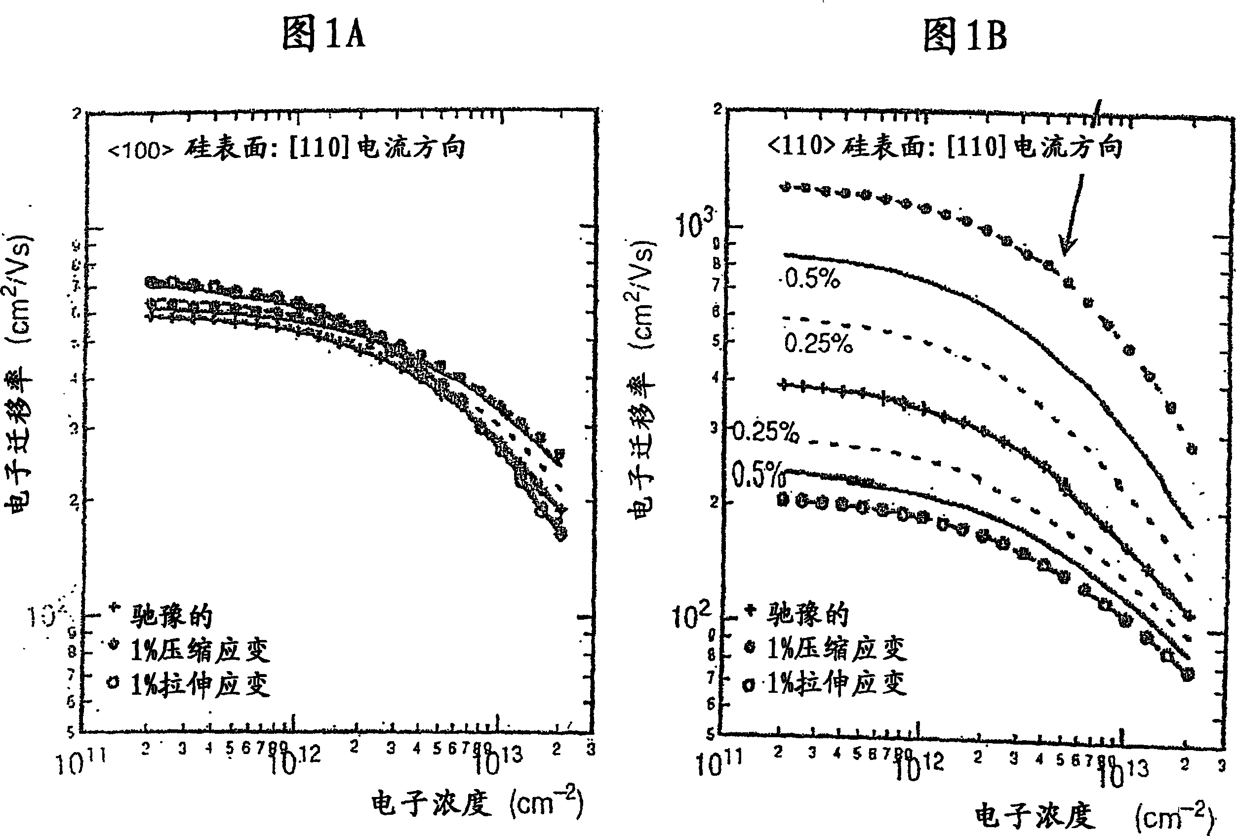
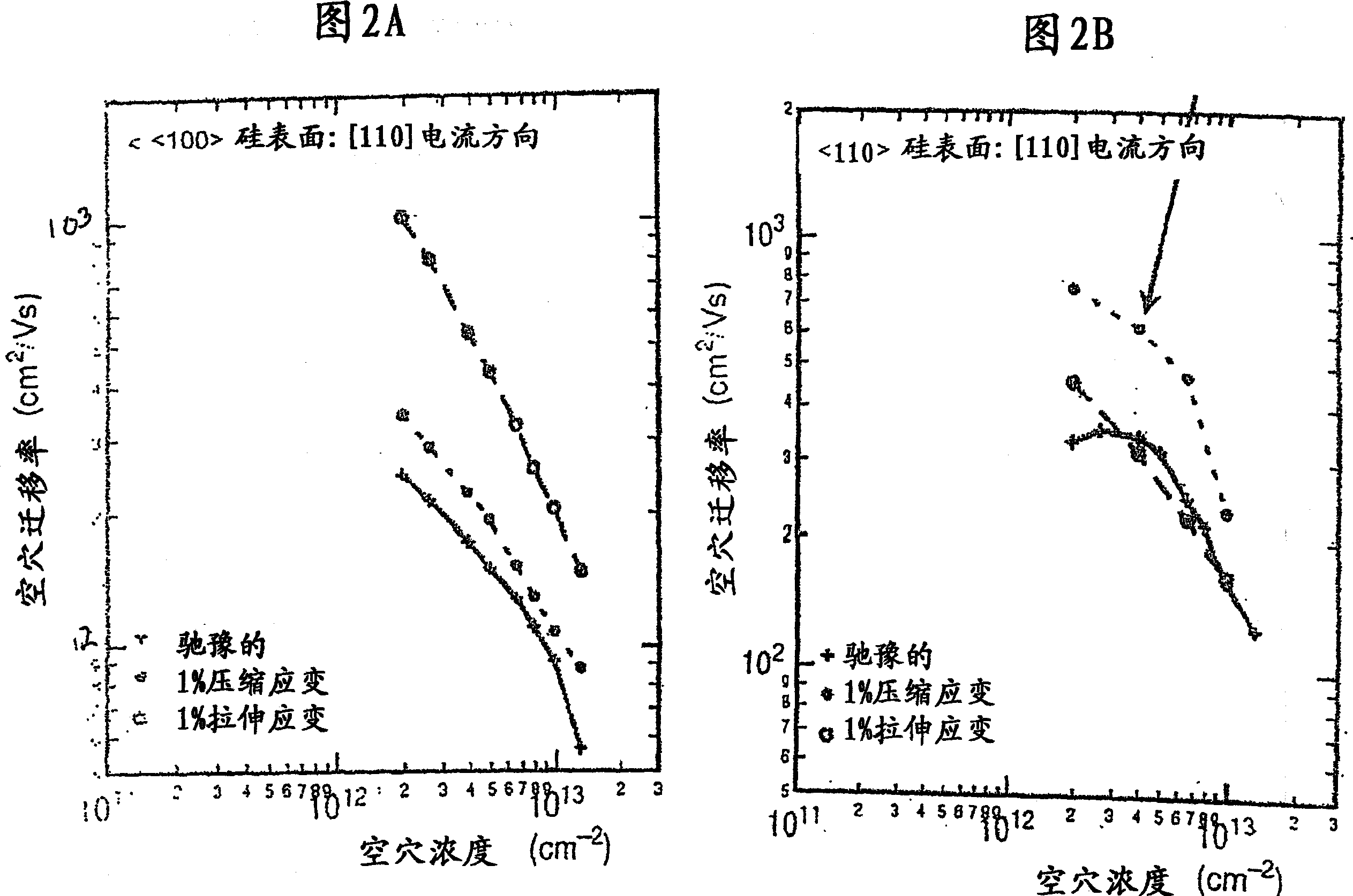
[0035] The present invention provides a semiconductor material comprising a silicon-containing layer having a crystal orientation and biaxial compressive strain, as well as various methods of forming the material, which will now be referred to by reference to the appended Fig. is described in more detail.

[0036] The applicants of the present application have determined by numerical calculations that when significant (greater than about 0.2%, preferably greater than about 0.5%) biaxial compressive strain is introduced onto a silicon-containing layer, electron and hole mobilities exceed conventional The case of unstrained silicon . Strain percent is defined herein as the percent change in the lattice constant of a material in a given direction. The significant advantages of the combination of biaxial compressive strain and silicon-containing layers have not previously been recognized in the art.

[0037] The results of the above calculations are shown in FIGS. 1A-1B and 2...


PUM

PropertyMeasurementUnit
thicknessaaaaaaaaaa
thicknessaaaaaaaaaa
depthaaaaaaaaaa

Abstract

The present invention provides a semiconductor material that has enhanced electron and hole mobilities that comprises a -containing layer having a 110 crystal orientation and a biaxial compressive strain. The term ''biaxial compressive stress'' is used herein to describe the net stress caused by longitudinal compressive stress and lateral stress that is induced upon the Si-containing layer during the manufacturing of the semiconductor material. Other aspect of the present invention relates to a method of forming the semiconductor material of the present invention. The method of the present invention includes the steps of providing a silicon-containing 110 layer; and creating a biaxial strain in the silicon-containing 110 layer.

Description

technical field [0001] The present invention relates to semiconductor materials having enhanced electron-hole mobility, and more particularly to semiconductor materials comprising silicon (Si)-containing layers having enhanced electron-hole mobility. The present invention also provides various methods of forming such semiconductor materials. Background technique [0002] For more than three decades, the continued miniaturization of silicon metal-oxide-semiconductor field-effect transistors (MOSFETs) has driven the semiconductor industry worldwide. For more than thirty years people have predicted fantastic gains in scaling, but a history of innovation has sustained Moore's Law despite many challenges. Today, however, there are increasing signs that metal-oxide-semiconductor (MOS) is starting to hit traditional scaling limits [A brief summary of the short- and long-term challenges to continued complementary metal-oxide-semiconductor scaling can be found at the International T...

Claims


Application Information

Patent Timeline
Patent Type & Authority Applications(China)
IPC IPC(8): H01L29/02H01L21/762H01L29/04
Inventor 陈永聪玛斯莫·V.·菲斯切特约翰·M.·赫根罗瑟杨美基拉杰施·仁加拉简亚历山大·里兹尼克保罗·所罗门宋均镛杨敏
Owner GLOBALFOUNDRIES INC
Why Eureka
Try Eureka