Liquid crystal display faceplate, and base plate of array in active mode

A technology for liquid crystal display panels and array substrates, which is used in static indicators, nonlinear optics, instruments, etc., can solve the problems of display screen flicker, unbalance, and reduce the display quality of the display panel, so as to reduce parasitic capacitance and improve quality. Effect

Inactive Publication Date: 2007-07-25
AU OPTRONICS CORP
View PDF0 Cites 28 Cited by
  • Summary
  • Abstract
  • Description
  • Claims
  • Application Information

AI Technical Summary

Problems solved by technology

[0016] In this way, the inconsistency of the feedthrough voltage ΔVp of each pixel causes the imbalance of the pixel voltage polarity reversal, and makes the gray scale voltage reference of each pixel have some errors, thus causing the human eye to observe the flickering phenomenon of the display screen, and Reduce the display quality of the display panel

Method used


Image

  • Liquid crystal display faceplate, and base plate of array in active mode
  • Liquid crystal display faceplate, and base plate of array in active mode
  • Liquid crystal display faceplate, and base plate of array in active mode

Examples


Embodiment Construction

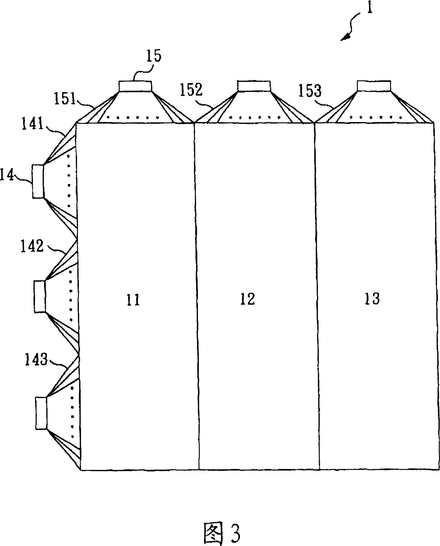
[0053] First, please refer to FIG. 3 and FIG. 4A, FIG. 4B, and FIG. 4C, wherein FIG. 3 is a schematic diagram showing sub-regions, and FIG. 4A, FIG. 4B, and FIG. 4C show a preferred embodiment of the present invention.

[0054] The lower substrate (not shown) of the liquid crystal display panel 1 is divided into display sub-regions 11, 12, 13, and the three display sub-regions respectively have a plurality of pixels 21, pixels 22 and pixels 23, and a plurality of gate driver chips 14, and a plurality of source driver chips 15, and in this embodiment, the projected areas of the display sub-regions 11, 12, and 13 are all the same.

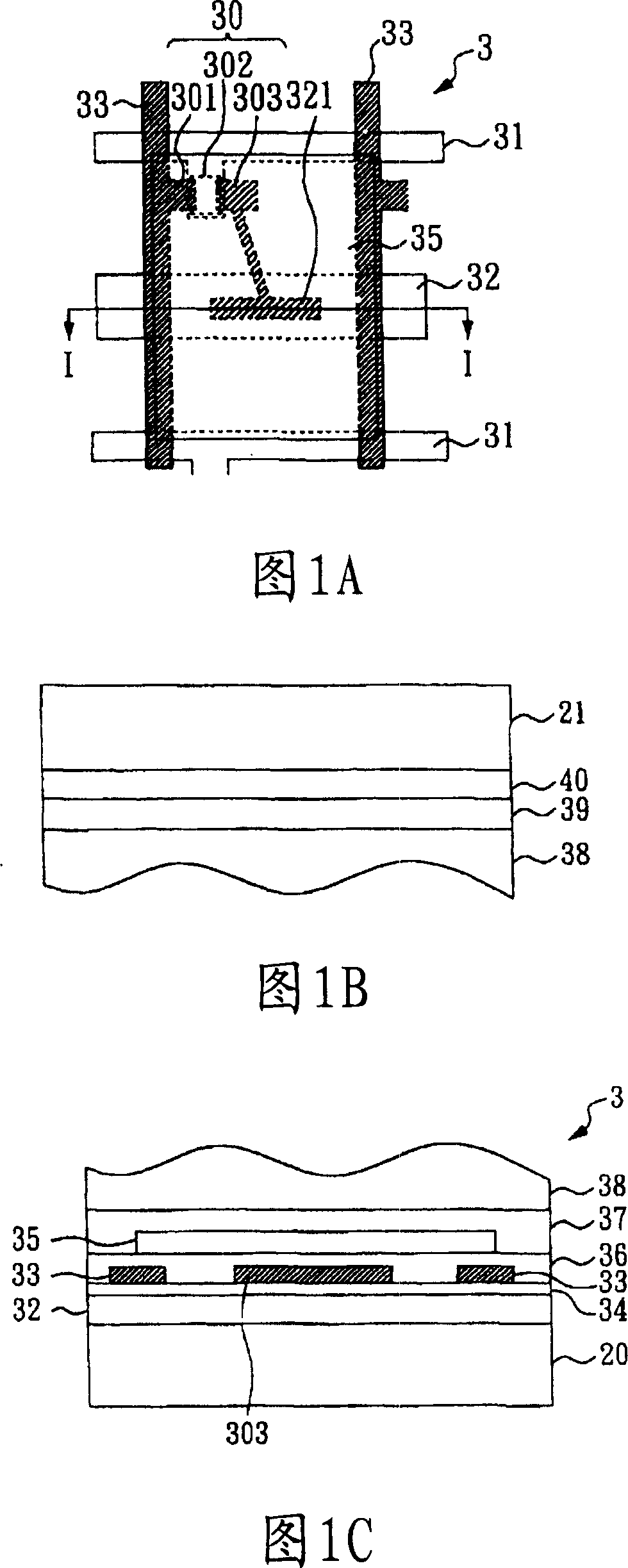
[0055] The pixels 21 , 22 , 23 respectively have a thin film transistor 30 and pixel electrodes 211 , 221 , 231 . The thin film transistor 30 includes a source 301 , a gate 302 , and a drain 303 . Moreover, the pixels 21, 22, 23 are electrically connected to the gate driver chip 14 through the gate 302 via the gate lines 141, 142, 143, and the pixels...


PUM


Abstract

A liquid crystal display faceplate is featured as decreasing parasitic capacity, liquid crystal capacity and / or auxiliary capacity by reducing projection area of pixel electrode in each display sub-region in sequence and carrying out capacity compensation on feed-through voltage by decreasing general capacity value of each pixel progressively in sequence for making feed-through voltage of said faceplate be more consistent so as to improve quality of displayed picture.

Description

technical field [0001] The invention relates to a liquid crystal display panel and an active array substrate, in particular to a thin film transistor liquid crystal display panel and an active array substrate. Background technique [0002] Please refer to FIG. 1A and FIG. 1B together. FIG. 1A shows a schematic diagram of a pixel of a traditional TFT-LCD panel, and FIG. 1B and 1C show a cross-sectional view of a pixel of a traditional TFT-LCD panel corresponding to the line segment I-I in FIG. 1A. [0003] Now use FIG. 1C to introduce the structure of the traditional active array substrate: firstly, on the lower substrate 20, the graphics of the gate line (Gate Line) 31 and the storage capacitor line (Storage Capacitor Line) 32 are made together; secondly, the insulating film is made 34. Afterwards, a source line (Source Line) 33, an organic layer (Organic Layer) 36, a pixel electrode (Pixel Electrode) 35, and finally a layer of alignment film (Alignment Film) 37 are fabricat...

Claims


Application Information

Patent Timeline
Patent Type & Authority Applications(China)
IPC IPC(8): G02F1/1362G02F1/133G09G3/36
Inventor 王净亦
Owner AU OPTRONICS CORP
Why Eureka
Try Eureka