Method and device for encapsulating electronic components with a conditioning gas

A technology of electronic components and packaging devices, which is applied in the field of packaging electronic components, can solve the problems of unusable mold parts, product loss, and the process of adhesion growth cannot be completely predicted and understood, and achieve the effect of preventing cooling

Active Publication Date: 2007-08-15
BESI NETHERLANDS BV
View PDF1 Cites 2 Cited by
  • Summary
  • Abstract
  • Description
  • Claims
  • Application Information

AI Technical Summary

Problems solved by technology

Current solutions for limiting the adhesion between encapsulation material and mold parts, as the method and device described in the preamble, are: that undesired adhesion can still develop to higher values, during use The process of adhesion growth cannot be fully predicted and understood, mold parts are unusable part of the time and product loss occurs

Method used


Image

  • Method and device for encapsulating electronic components with a conditioning gas
  • Method and device for encapsulating electronic components with a conditioning gas

Examples


Embodiment Construction

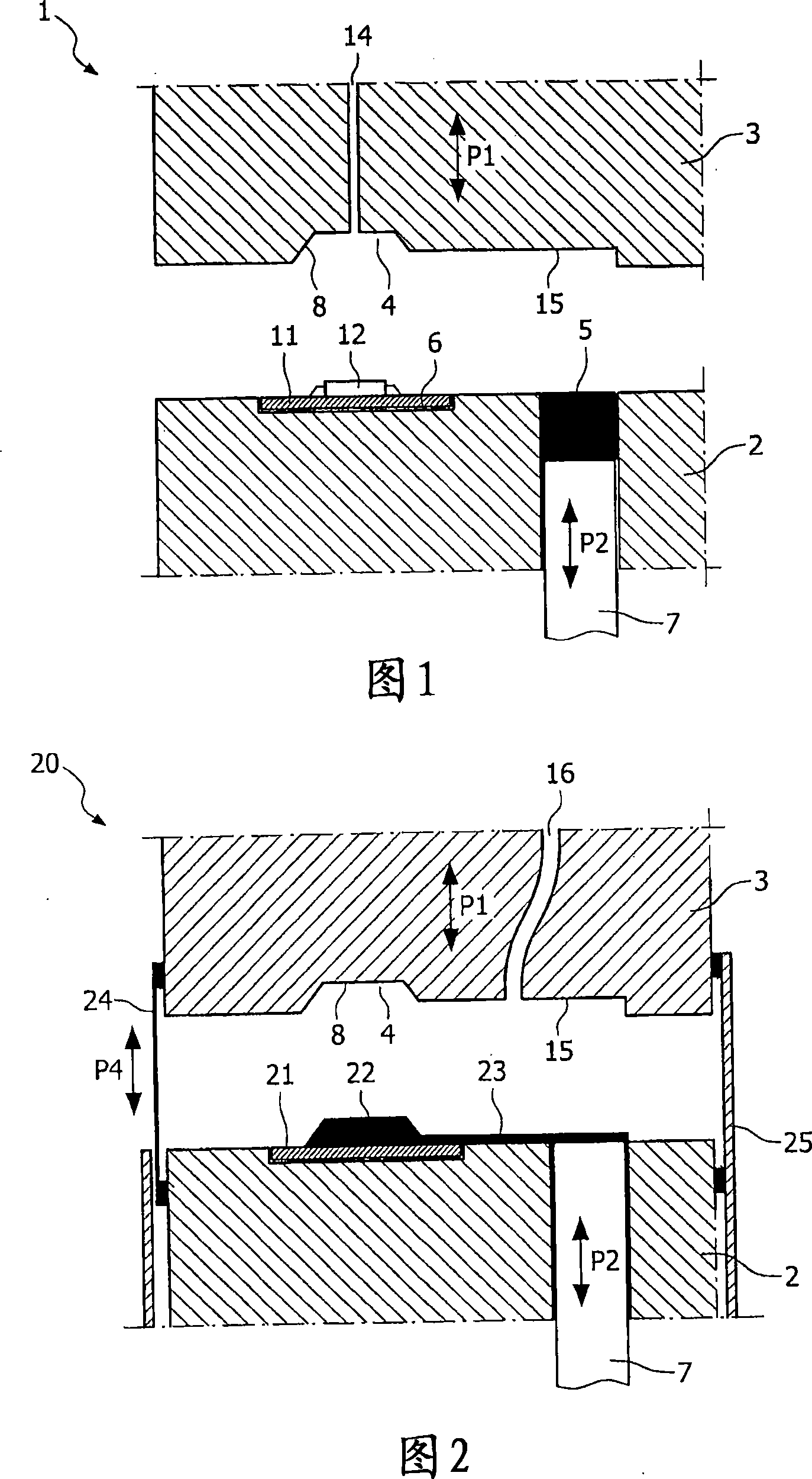
[0021] Figure 1 shows a packaging device 1 having a lower end-mold part 2 which is replaceable with respect to an upper end-mold part 3, as indicated by arrow P1. To form a housing, which is produced from a potting material 5 , the upper mold part 3 has a mold cavity 4 , not shown in this figure, which is clearly visible on the left. In the lower end mold part 2 a recess 6 is provided, on which a carrier with electronic components 12 is placed. The encapsulating material 5 can be applied to the mold cavity 4 via a replaceable plunger 7 as indicated by the arrow P2. Recessed into the upper mold part 3 is an optionally closeable channel 14 connected to the mold cavity 4 . The conditioning gas is fed directly into the mold cavity 4 via the channel 14 and at the same time exerts (at least partially acts on) a force on the encapsulation material 5 in order to release the encapsulation material 5 from the contact side 8 of the mold cavity 4 .

[0022] FIG. 2 shows a packaging devi...


PUM


Abstract

The invention relates to a method for encapsulating electronic components in a mould (2, 3) by the processing steps of: A) placing the electronic component (12) for encapsulating in a mould cavity (4), and B) feeding an encapsulating material (5) to the mould cavity (4), wherein at least a part of the mould surface (8) defining the mould cavity (4) is brought into contact with a conditioning gas containing a decreased oxygen concentration relative to the atmosphere. The device also relates to a device for encapsulating an electronic component (12), in particular a semiconductor, with encapsulating material.

Description

technical field [0001] The invention relates to a method for encapsulating electronic components in a mold according to the preamble of claim 1 . The invention also relates to a device for encapsulating an electronic component, in particular a semiconductor, with an encapsulating material according to the preamble of claim 12 . Background technique [0002] The packaging of electronic components, such as especially semiconductor circuits, is used extensively. The electronic component is here typically mounted on a carrier ("leadframe", "board") which is clamped between the parts of the mold so that it surrounds the The electronic components on the carrier form a mold cavity. An important consideration here is that the mold must maintain limited adhesion to the encapsulation material in order to prevent damage to the packaged product and contamination of the mold during processing of the encapsulation material. To limit the degree of adhesion between the encapsulation mate...

Claims


Application Information

Patent Timeline
Patent Type & Authority Applications(China)
IPC IPC(8): B29C45/43B29C45/14B29C39/42B29C33/70B29C33/10B29C33/58B29C33/60B29C45/02
CPCB29C39/42B29C45/43B29C2791/005B29C45/1701B29C33/70B29C33/58B29C45/14655B29C33/60B29C33/10B29C33/46B29C45/02B29C45/14
Inventor H·J·B·彼得斯A·T·J·赖梅尔F·B·A·德弗里斯J·L·G·M·芬罗伊
Owner BESI NETHERLANDS BV
Why Eureka
Try Eureka