

Signal shaping process and its device
A signal shaping and signal technology, applied in pulse shaping and other directions, can solve the problems of memory read and write confusion, input signal glitches, abnormal circuit functions, etc., to achieve the effect of simplifying the design
Patent Information
- Authority / Receiving Office
- CN · China
- Patent Type
- Applications(China)
- Current Assignee / Owner
- Publication Date
- 2007-09-19
- Estimated Expiration
- Not applicable · inactive patent
Smart Images
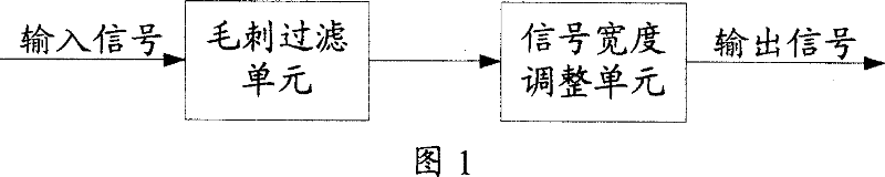
Figure 1 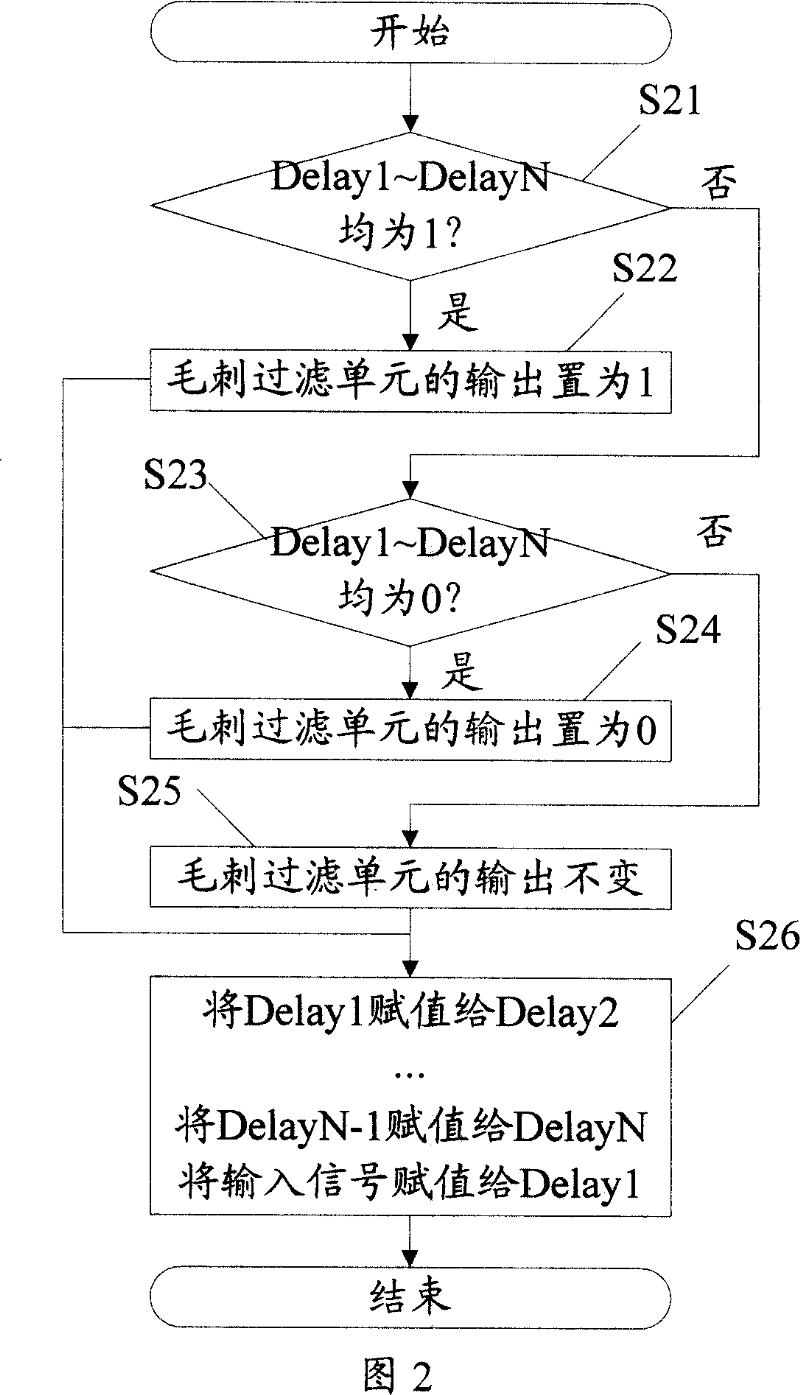
Figure 2 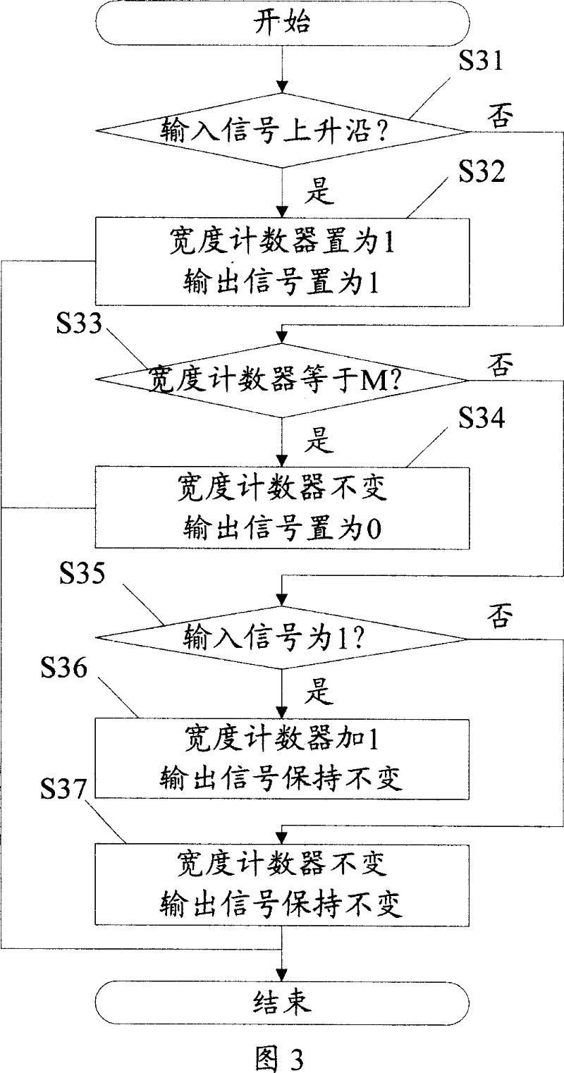
Figure 3
Abstract
Description
technical field
[0001] The invention relates to digital signal processing technology, in particular to a signal shaping method and device. Background technique
[0002] At present, the integrated circuit industry is in a stage of rapid development, and the application range of integrated circuit products is becoming wider and wider. Accompanied by the environment that integrated circuit products need to adapt to is becoming more and more complex, so the environmental adaptability of integrated circuit products put forward higher requirements.
[0003] There are many interferences in the real environment, such as EMI interference, radiation interference, etc. These interferences will greatly affect the signal integrity, resulting in the introduction of burrs on the input signal or unpredictable changes in the format of the input signal. These unpredictable changes may lead to abnormal circuit functions, especially in circuits that need to store input data in a certain format...
Examples
Embodiment Construction
[0017] The signal shaping method and device thereof of the present invention will be further described in detail below in conjunction with the accompanying drawings. To simplify the description, the signal width referred to below is in the unit of the number of clocks, and it is assumed that the input signal is active high.
[0018] Referring to FIG. 1 , the signal shaping device of the present invention is composed of a glitch filtering unit 1 and a signal width adjusting unit 2 . The input signal is output to a subsequent circuit part (not shown) via the glitch filter unit 1 and the signal width adjustment unit 2 in sequence.
[0019] Glitch filtering unit 1 is used to filter the burrs in the input signal, such as: jitter, noise, etc., according to the minimum effective width L of the input signal min , set an appropriate burr width N, so that N satisfies: 0min . If the effective width of the input signal is less than N clocks, filter out the segment of the input signal as...