Phase change memory cell employing a gebite layer as a phase change material layer, phase change memory device including the same, electronic system including the same and method of fabricating the sa
What is AI technical title?
AI technical title is built by PatSnap AI team. It summarizes the technical point description of the patent document.
一种相变存储、器件的技术,应用在相变存储器,电子系统领域,能够解决妨碍GeSbTe层晶化等问题
Inactive Publication Date: 2007-11-21
SAMSUNG ELECTRONICS CO LTD
View PDF2 Cites 8 Cited by
Summary
Abstract
Description
Claims
Application Information
AI Technical Summary
This helps you quickly interpret patents by identifying the three key elements:
Problems solved by technology
Method used
Benefits of technology
Problems solved by technology
However, impurities in the GeSbTe layer prevent the GeSbTe layer from being crystallized
Method used
Image
Click on the blue label to locate the original text in one second.
Reading with bidirectional positioning of images and text.
Examples
Embodiment Construction
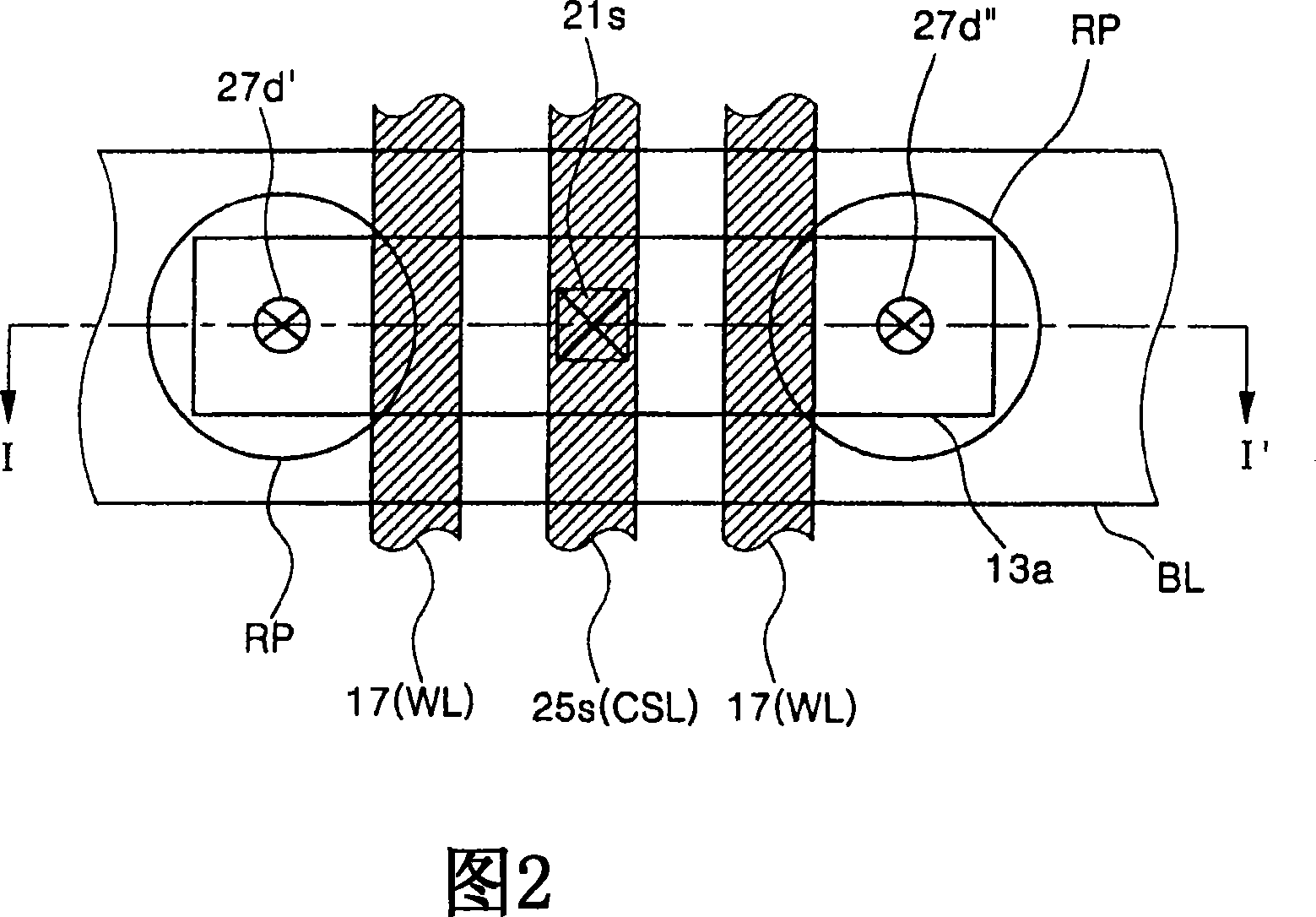
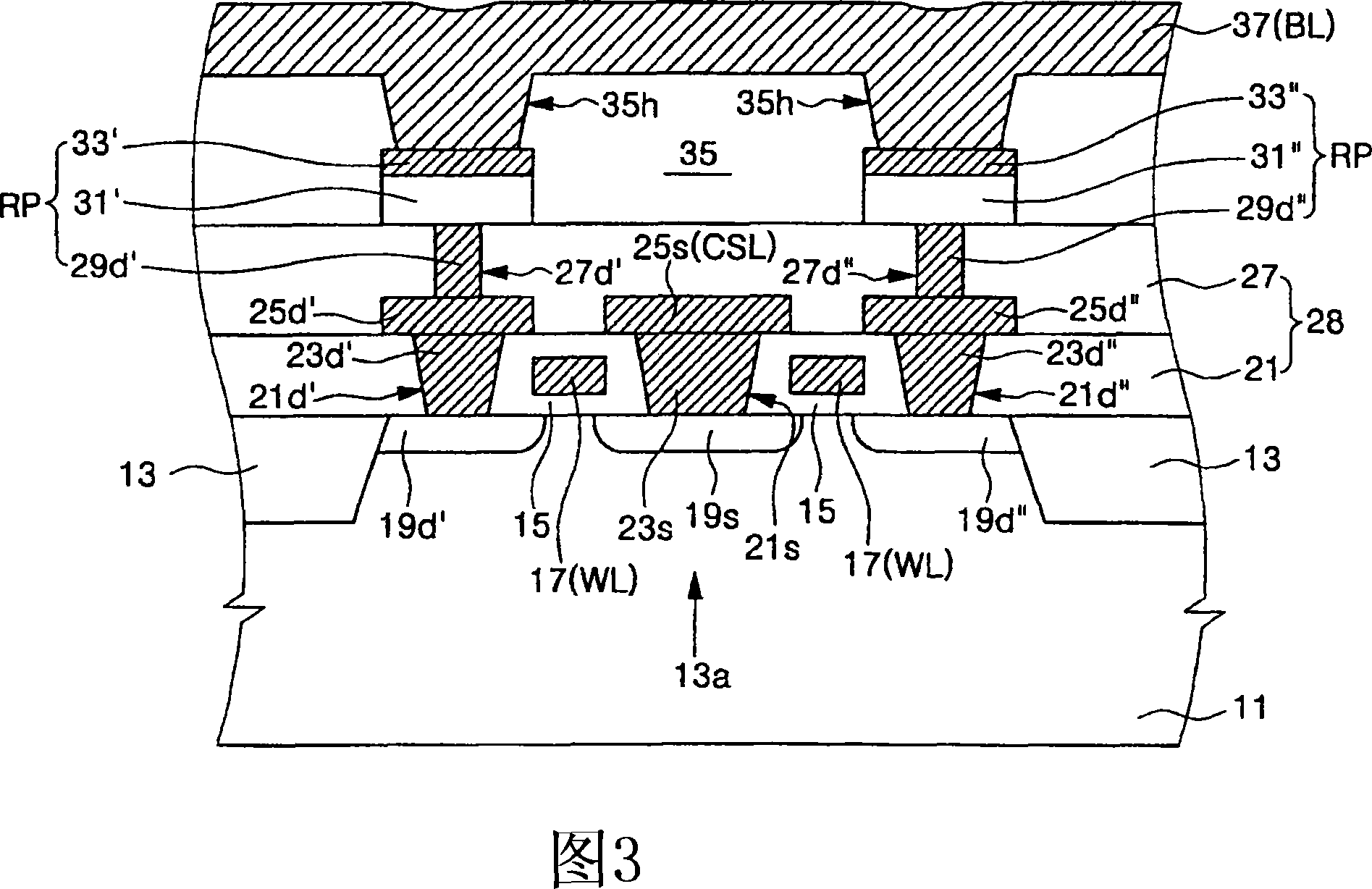
[0042] The present invention will now be described more fully with reference to the accompanying drawings, in which preferred embodiments of the invention are shown. This invention may, however, be embodied in different forms and should not be construed as limited to the embodiments set forth herein. Rather, these embodiments are provided so that this disclosure will be thorough and complete, and will fully convey the scope of the invention to those skilled in the art. In the drawings, the thickness of layers and regions are exaggerated for clarity. Throughout the specification, like symbols refer to like elements.
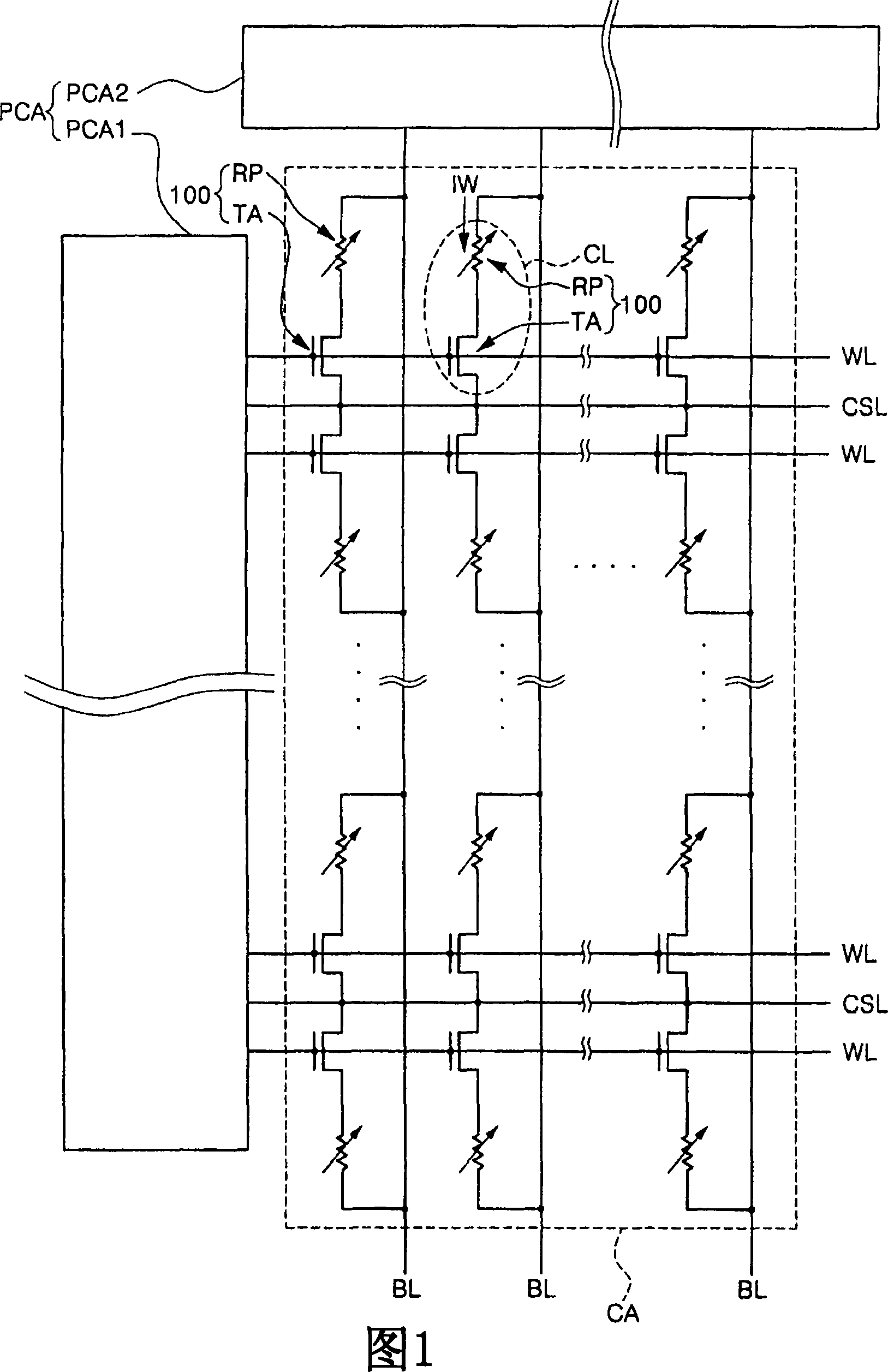
[0043] FIG. 1 is a schematic block diagram of a phase change memory device employing a phase change memory cell according to an exemplary embodiment of the present invention.
[0044] Referring to FIG. 1, the phase change memory device includes a cell array area CA and a peripheral circuit area PCA. The cell array area CA, ie, the memory cell area, includes a p...
PUM
Abstract
A phase change memory cell includes an interlayer insulating layer formed on a semiconductor substrate, and a first electrode and a second electrode disposed in the interlayer insulating layer. A phase change material layer is disposed between the first and second electrodes. The phase change material layer may be an undoped GeBiTe layer, a doped GeBiTe layer containing an impurity or a doped GeTe layer containing an impurity. The undoped GeBiTe layer has a composition ratio within a range surrounded by four points (A 1 (Ge21.43, Bi16.67, Te61.9), A 2 (Ge44.51, Bi0.35, Te55.14), A 3 (Ge59.33, Bi0.5, Te40.17) and A 4 (Ge38.71, Bi16.13, Te45.16)) represented by coordinates on a triangular composition diagram having vertices of germanium (Ge), bismuth (Bi) and tellurium (Te). The doped GeBiTe layer contains an impurity and has a composition ratio within a range surrounded by four points (D 1 (Ge10, Bi20, Te70), D 2 (Ge30, Bi0, Te70), D 3 (Ge70, Bi0, Te30) and D 4 (Ge50, Bi20, Te30)) represented by coordinates on the triangular composition diagram.
Description
[0001] Cross References to Related Applications [0002] This application claims priority to Korean Patent Application No. 2006-45298 filed on May 19, 2006, the disclosure of which is hereby incorporated by reference in its entirety. technical field [0003] The present invention relates to a non-volatile memory, and more specifically, to a phase-change memory unit using a GeBiTe layer as a phase-change material layer, a phase-change memory including the phase-change memory unit, an electronic system including the phase-change memory and a manufacturing method thereof . Background technique [0004] Nonvolatile memories retain their stored data even when their power supply is cut off. Therefore, nonvolatile memories are widely used in computers, mobile telecommunication systems, memory cards, and the like. [0005] A flash memory is widely used as a nonvolatile memory. Many flash memories employ memory cells with a stacked gate structure. The stacked gate structure of a ...
Claims
Application Information
Patent Timeline
Application Date:The date an application was filed.
Publication Date:The date a patent or application was officially published.
First Publication Date:The earliest publication date of a patent with the same application number.
Issue Date:Publication date of the patent grant document.
PCT Entry Date:The Entry date of PCT National Phase.
Estimated Expiry Date:The statutory expiry date of a patent right according to the Patent Law, and it is the longest term of protection that the patent right can achieve without the termination of the patent right due to other reasons(Term extension factor has been taken into account ).
Invalid Date:Actual expiry date is based on effective date or publication date of legal transaction data of invalid patent.

