Process for producing nano-scale cross lines array structure organic molecule device

A technology of molecular devices and array structures, applied in semiconductor/solid-state device manufacturing, semiconductor devices, electric solid-state devices, etc., can solve the problems of polluting organic materials, difficult processing, and improvement, and achieve the effect of avoiding damage and improving reliability

Active Publication Date: 2007-12-05
SEMICON MFG INT (SHANGHAI) CORP +1
View PDF0 Cites 6 Cited by
  • Summary
  • Abstract
  • Description
  • Claims
  • Application Information

AI Technical Summary

Problems solved by technology

The current manufacturing process of the cross-wire structure is generally to first prepare the lower electrode, then grow the organic material, and finally complete the preparation of the upper electrode. In the prepar

Method used


Image

  • Process for producing nano-scale cross lines array structure organic molecule device
  • Process for producing nano-scale cross lines array structure organic molecule device
  • Process for producing nano-scale cross lines array structure organic molecule device

Examples


Embodiment Construction

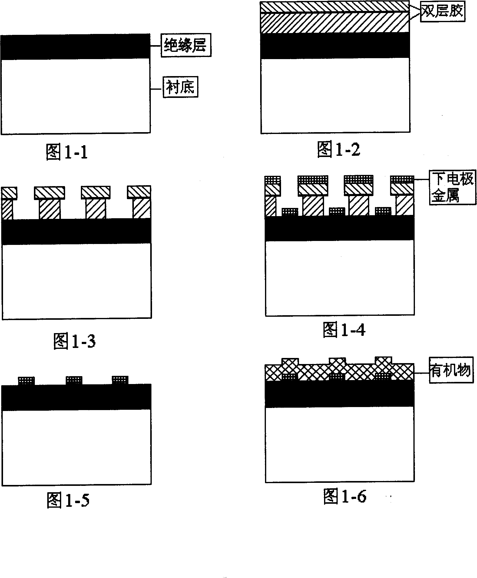
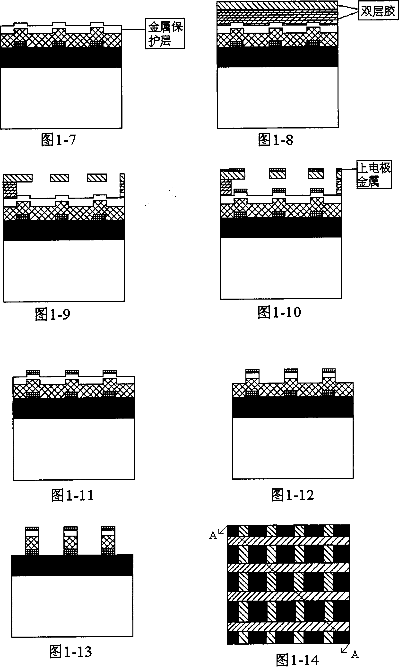
[0015] Invention flow chart (the section selected in the flow chart is the A-A section in Figure 1-14):

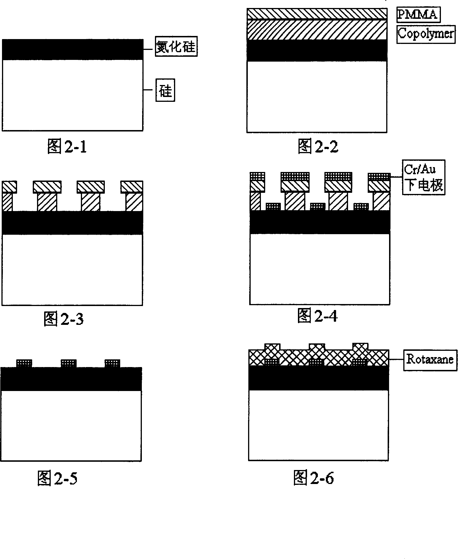
[0016] 1. As shown in Figure 1-1, an insulating layer film is prepared on the substrate surface by thermal oxidation growth or chemical vapor deposition.

[0017] 2. As shown in Figure 1-2, spin-coat electron beam photoresist on the surface of the insulating layer film, and bake it on a hot plate or an oven.

[0018] 3. As shown in Figure 1-3, the lower electrode pattern is obtained on the photoresist after electron beam exposure and development.

[0019] 4. As shown in Figure 1-4, the metal thin film of the lower electrode is obtained by metal evaporation.

[0020] 5. As shown in Figure 1-5, the metal lower electrode is prepared on the insulating layer after ultrasonic stripping with acetone, ethanol and deionized water.

[0021] 6. As shown in Figure 1-6, the organic molecular film is prepared by vacuum evaporation or liquid phase LB film. Organic molecular materials ...


PUM


Abstract

The invention belongs to the micro machining field in microelectronics and molectronics, especially relating to a method for preparing nano cross line array structure organic molecular device, comprising the steps of: 1. depositing insulating film on substrate surface; 2. spin-coating electron beam resist on the insulating film surface, making electron beam exposure and developing to obtain lower electrode figure; 3. evaporating to prepare lower electrode metal; 4. peeling off the metal to obtain cross line lower electrode; 5. cover-grow organic molecular film on the lower electrode; 6. evaporating to prepare metal protection layer on the organic molecular film; 7. spin-coating double layers of photoetching glue on the protection layer, and making electron beam exposure and developing to obtain upper electrode figure; 8. slantingly evaporating to prepare upper electrode metal film; 9. peeling off the metal to obtain cross line upper electrode; and 10. dry-etching the protection layer and completing preparing of the device.

Description

technical field [0001] The invention belongs to the field of microfabrication in microelectronics and molecular electronics, and in particular relates to a preparation method of an organic molecular device with a nanoscale cross-line array structure. Background technique [0002] As the feature size of large-scale integrated circuits enters the nanometer level, the traditional silicon-based integrated circuit technology is facing challenges, and the research on new materials and new structures has become a hot spot. Molecular electronic devices, one of the branches of nanoelectronics, are booming. FET and cross-wire are currently the main structures of molecular electronic devices, and the cross-wire structure is beneficial to integration and has attracted extensive attention. The current manufacturing process of the cross-wire structure is generally to first prepare the lower electrode, then grow the organic material, and finally complete the preparation of the upper electr...

Claims


Application Information

Patent Timeline
IPC IPC(8): H01L51/40
Inventor 商立伟涂德钰王丛舜刘明
Owner SEMICON MFG INT (SHANGHAI) CORP
Why Eureka
Try Eureka