Hinge concealed micro electromechanical device
A technology of micro-electromechanical devices and electrodes, which is applied in the field of forming integrated devices such as semiconductor devices, and can solve problems such as hinge elasticity, mirrors that cannot be completely flat, and mirror heights that are different
Inactive Publication Date: 2008-01-09
MICRONIC LASER SYST
3 Cites 0 Cited by
AI-Extracted Technical Summary
Problems solved by technology
However, using reflectors made of aluminum has some disadvantages such as: mirrors may not be perfectly flat; mirror heights may vary between mirrors; m...
Method used
[0035] In FIG. 17 the foot structure is released. An isotropic RIE of the substrate 130 (which could also be replaced by a wet isotropic or anisotropic etch) was performed by an under etch of the material between the hinges to free the bottom of the mirror. By removing material between the hinges, the applied actuation force to deflect the mirror into a deflected state can be greatly reduced. Isotropic etching also removes unnecessary material in the mirror, ie reduces its weight, which can affect the speed at which the mirror is put from one state to another and its own oscillation frequency.
[0046] FIG. 21 shows a perspective view of an exemplary embodiment of a mirror structure 132 according to the present invention. The mirror structure includes a mirror surface 135 , a support 134 , a cavity 131 , a base element 136 , a first leg 142 and a second leg 144 . The mirror structure 132 can have a pr...
Abstract
The invention provides a micro electromechanical device making method, comprising: removing material from a substrate to define at least a hidden support in the substrate; pasting at least a hidden support onto a chip including at least an actuation electrode, which can actuate at least a part of the substrate and the rotating axis of the substrate is basically vertical to the hidden support.
Application Domain
Optical elements
Technology Topic
Hinge angleEngineering +2
Image
Examples
- Experimental program(1)
Example Embodiment
[0017] For the purposes of this application, the terms "wafer" and "substrate" are used interchangeably, and the difference between them is only in their dimensions.
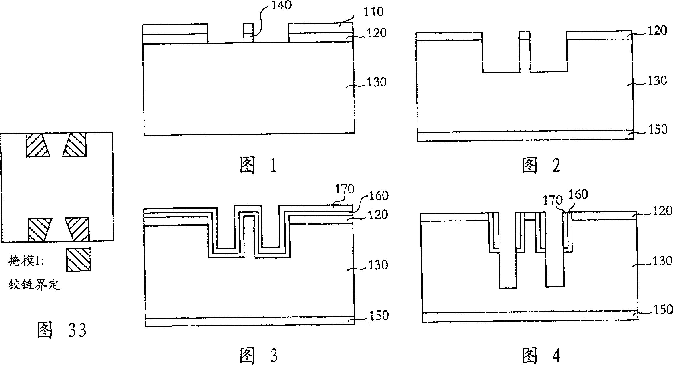
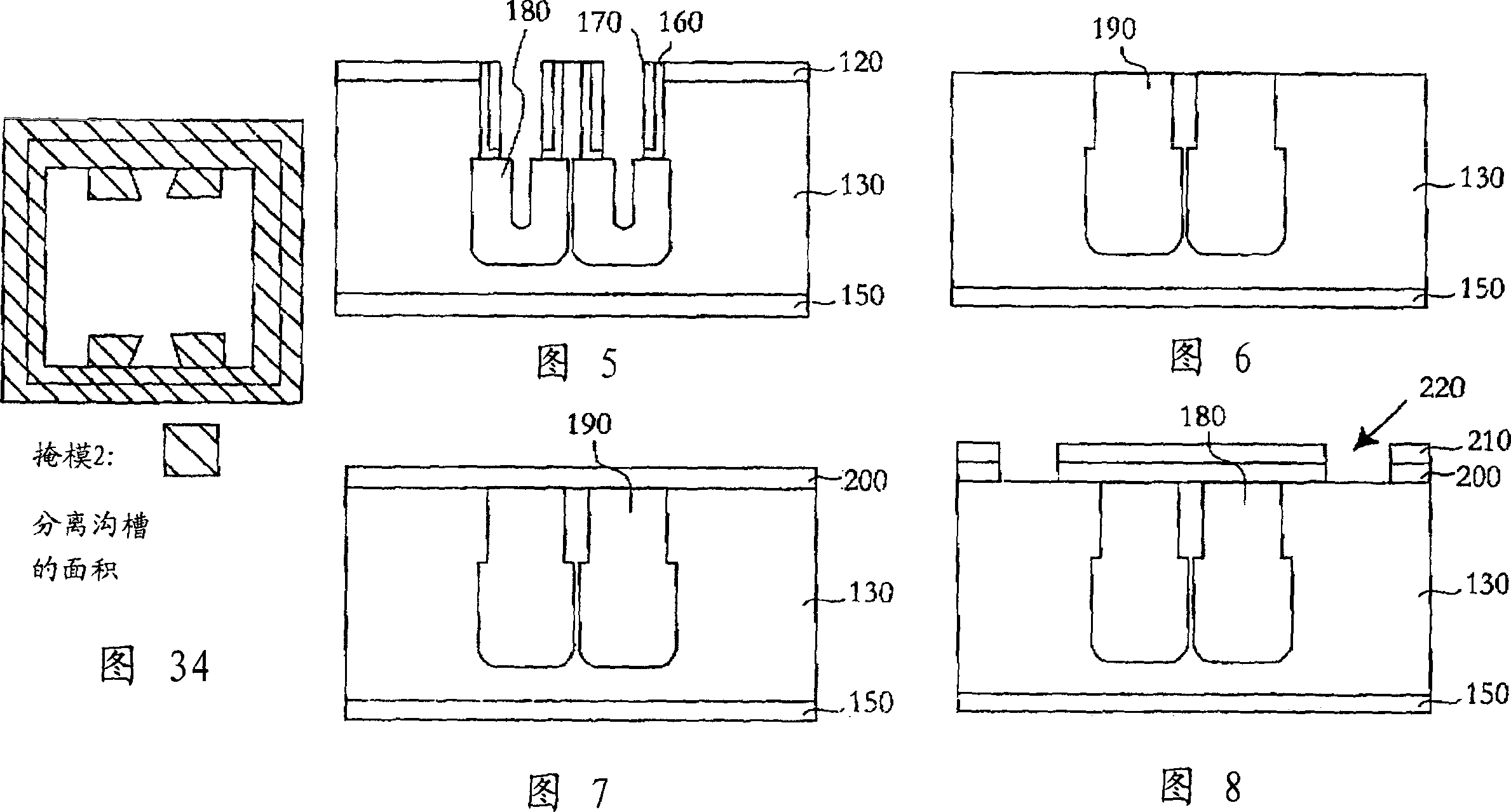
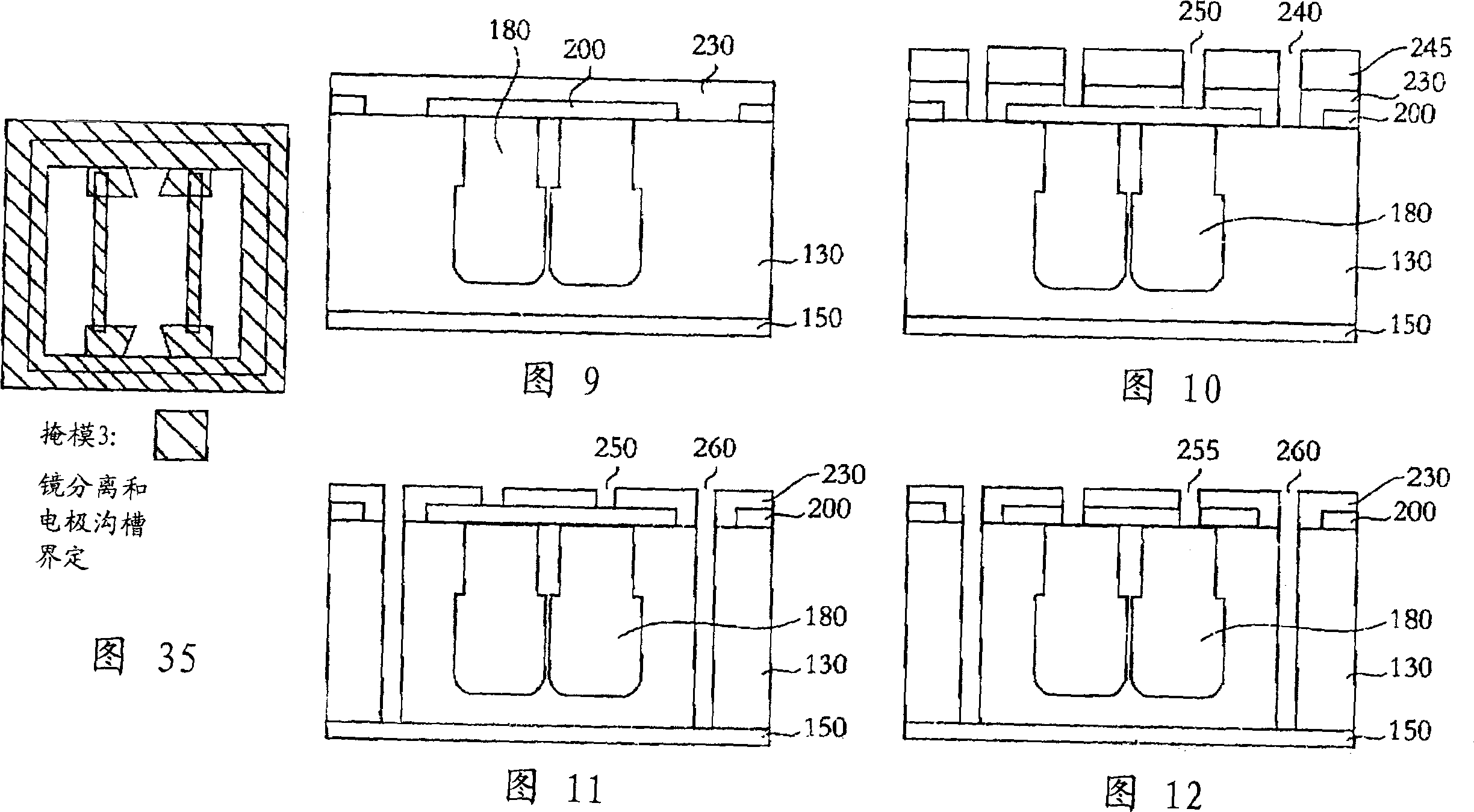
[0018] The method according to the invention is particularly suitable for manufacturing micromirror spatial light modulators. However, it can be applied to a variety of microelectromechanical devices, thermal detectors and non-thermal detector devices such as quantum well detectors, pyroelectric detectors, bolometers, etc., but is not limited thereto. The present invention is particularly applicable when a structure (such as a micromirror array) cannot be directly processed/patterned/deposited on a substrate with another structure (such as a steering electronic device). For example, this is the case if the structure provided on the substrate is sensitive to the process temperature of the processing of the structure to be provided thereon, or when the substrate is polycrystalline and the elements grown on the substrate must be single crystals.
[0019] Fig. 1 schematically shows a first process step according to an exemplary embodiment of the present invention for forming a MEMS device with a hidden hinge. The hidden hinge is a hinge that is hidden by a reflective surface in the MEMS device when the MEMS device is viewed from above, for example, the top. The starting material is wafer 130, which is made of single crystal silicon or SOI (Silicon On Insulator). A mask material layer 120 such as silicon oxide is provided on top of the wafer 130. The mask material layer 120 may be at least partially covered by the resist film 110. In the first process step, a standard photolithography process can be used to define the hinge 140 in the mask material 120. Can be CF 4 The reactive ion etching RIE can be used to remove exposed areas of the resist film 110 and the underlying mask material 120.
[0020] The definition of the hinge in the substrate 130 can be performed by using deep reactive ion etching (DRIE) (FIG. 2). Before the hinge is defined in the substrate 130, the resist film 110 may be removed in a resist remover. Before the hinges in the substrate 130 are defined, the substrate may be immersed in 2% HF. DRIE may be a well-known Bosch process. The most simplified process involves only anisotropic DRIE etching, followed by isotropic RIE to form the hinge. Before the hinge in the substrate 130 is defined, a silicon oxide layer 150 may be disposed on the opposite side of the substrate 130 with respect to the hinge. Alternatively, the silicon oxide layer 150 may be in the substrate 130. The hinge is defined on the opposite side.
[0021] In the next step, passivation of the treated surface can be performed (Figure 2). Dry oxidation can be performed to relieve stress in the silicon during local oxidation (not shown in Figure 3). The oxidation is optional to improve accuracy and reduce surface roughness. PECVD (plasma enhanced chemical vapor deposition) of silicon nitride can be performed as an oxidation barrier in the subsequent LOCOS (local oxidation of silicon) step. PECVD of the silicon oxide 170 as an etching protection can be performed as a protection in the subsequent DRIE step.
[0022] In FIG. 4, the passivation layer (silicon nitride 160 and silicon oxide 170) on the horizontal surface is removed, and the length of the hinge in the substrate 130 is defined. The passivation layer can be removed by a high directivity (low voltage and high radio frequency power) RIE method. The exposed surface of the substrate 130 can be etched by a DRIE (Bosch process) method to define the length of the hinge.
[0023] In the next step, as shown in Figure 5, thermal oxidation is performed to define the width of the hinge. LOCOS can be used to convert part of the substrate 130 in the hinge into silicon oxide 180.
[0024] In FIG. 6, the passivation layer and mask material are removed and the substrate is planarized. The passivation layers 160, 170, 180 and the mask material 120 may be etched away in BOE (Buffer Oxidation Etching). Polyimide (PI) 190 may be applied rotatably on the top of the substrate 130 to fill the cavity therein. A reduced pressure or vacuum can be used to ensure that the PI will fill the cavity. The PI can be hardened at an elevated temperature. Can use O 2 The plasma removes undesirable PI.
[0025] A mask material 200 is deposited on top of the substrate 130 (FIG. 7). The mask material may be aluminum and may be deposited by evaporation.
[0026] On top of the mask material, a resist film may be provided. Standard lithography can define a region 220 in the substrate 130 where the mirror separation trench will be defined (see FIG. 8). The aluminum under the exposed resist can be passed through RIE (SiCL 4 /Cl 2 ) To remove. It is also possible to form the separation trench as the first step of trench isolation for electronic devices by using an SOI wafer with trenches (usually filled with oxide).
[0027] The unexposed resist film can be removed by acetone. On top of the mask material 200 and the released substrate 130, a silicon oxide layer is provided (see FIG. 9). The layer can be provided by PECVD method.
[0028] On top of the silicon oxide layer 230, a resist layer 245 is provided. Standard photolithography may define the mirror separation trench 240 and the electrode trench 250 in the mask material 230 (silicon oxide). Silicon oxide 230 can be passed through, for example, CF 4 RIE method etching.
[0029] In FIG. 11, the mirror separation trench 260 has been formed in the substrate 130. The resist 245 has been removed by using, for example, acetone. The mirror trench 260 in the substrate 130 may be formed by using a Bosch process.
[0030] In Figure 12, electrode trenches 255 in the aluminum layer have been defined. The electrode trench can be passed through, for example, SiCl 4 /Cl 2 The RIE method is defined.
[0031] The PI has been introduced into the mirror groove 260 in FIG. 13. Unwanted PI can be used by using O 2 The plasma is removed.
[0032] The electrode trench 257 has been formed in the substrate 130 in FIG. 14. The electrode trench 257 may be formed by using a Bosch process.
[0033] In FIG. 15, silicon oxide 270 has been deposited by plasma enhanced chemical vapor deposition as an etch protection in the subsequent isotropic DRIE step.
[0034] In FIG. 16, the passivation layer 270 on the horizontal surface has been removed. The passivation layer can be removed by using RIE.
[0035]In Fig. 17 the foot structure is released. The isotropic RIE of the substrate 130 (which can also be replaced by wet isotropic or anisotropic etching) is performed by etching down the material between the hinges to release the bottom of the mirror. By removing the material between the hinges, the actuation force applied to deflect the mirror to a certain deflection state can be greatly reduced. Isotropic etching also removes unnecessary materials in the mirror and reduces its weight, which can affect the speed of the mirror from one state to another and its own oscillation frequency.
[0036] In FIG. 18, the passivation layers 230, 270 and the mask layer 200 have been removed. These layers can be removed by the BOE method.
[0037] In FIG. 19, the substrate 300 with the actuation electronic device 310 has been attached to the substrate 130. At least one hinge is attached to the base plate 300. The substrate 300 has a raised structure 320 for attaching the hinge (alternatively, the electrode area of the substrate 130 can be lowered). In addition to the elevated structure 320, an actuation electronic device 310 is provided. It can be easily seen here that there is a large attachment area where the substrate 130 is attached to the substrate 300. Even if there is a slight mismatch between the two substrates, successful attachment can still be performed. The attachment may be low-temperature oxygen plasma assisted bonding, adhesive bonding (gluing), soldering, eutectic welding, fusion welding (direct bonding), glass glaze bonding, and anode bonding.
[0038] In FIG. 20, the buried oxide 280 has been removed from the substrate 130. The buried oxide can be removed by the BOE method. The mirror 132 can be released by removing the PI. PI can be used by O 2 The plasma is removed. It can be seen from Figure 20 that the mirror structure is quite rigid. This is due to the vertical portion 136 that will greatly affect the rigidity and flatness of the mirror surface. The hinge 134 can be designed to be hard or soft as desired. The mirror can be made of pure single crystal material, such as silicon. Other optional materials for the mirror can be polysilicon, quartz, III-V group materials, SiC. In order to increase the electrical conductivity, if the mirror material is formed of a semiconductor material, the mirror material may be doped. The surface facing the electronic device in the substrate 300 may be coated with a conductive material.
[0039] 22-32 illustrate another alternative embodiment of the manufacturing process of the MEMS device of the present invention. In FIG. 22, the starting material is a wafer 130, which may be made of single crystal silicon or SOI. A mask material layer 120 such as silicon oxide is provided on the surface of the wafer 130. The mask material 120 may be at least partially covered by the resist film 110. In the first process step, a standard photolithography process can be used to define the trench isolation 300 in the mask material 120. Can be CF 4 RIE (Reactive Ion Etching) may be used to remove exposed areas of the resist film 110 and the underlying mask material 120.
[0040] The trench isolation definition in the substrate 130 can be performed by DRIE (deep RIE). Before the trench isolation 300 is defined in the substrate 130, the resist film 110 may be removed in a resist remover. Before the hinges in the substrate 130 are defined, the substrate may be immersed in 2% HF. DRIE may be a well-known Bosch process. The most simplified process includes only anisotropic DRIE etching, followed by isotropic RIE to form the trench. Before defining the trench in the substrate 130, a silicon oxide layer 150 may be provided on the opposite side of the substrate 130 from where the trench 300 will be defined. Alternatively, the silicon oxide layer 150 may be provided on the substrate 130. After defining the groove in the middle, it is disposed on the opposite side.
[0041] The trench 300 may be filled by first rotatingly applying polyimide (PI) 310 on the top of the substrate 130 to fill the cavity therein. A reduced pressure or vacuum can be used to ensure that the PI will fill the cavity. The PI can be hardened at elevated temperatures. Unwanted PI can use O 2 Plasma removal, see Figure 24.
[0042] Figures 25-29 show the process steps used to define buried or hidden hinges. In FIG. 25, standard photolithography may be used to define the entrance hole 310 in the mask material 120. Can be CF 4 RIE (Reactive Ion Etching) may be used to remove exposed areas of the resist film 110 and the underlying mask material 120.
[0043] In FIG. 26, dry etching may be used to define holes 320 in the substrate 130. After the holes have been defined in the substrate 130, peeling of the resist 110 may be performed. After the resist is stripped, an oxide layer may be deposited to provide the oxide layer in the hole 320.
[0044] In FIG. 27, dry etching may be used to etch the horizontal surface of the oxide layer.
[0045] In FIG. 28, isotropic dry etching may be used to create a cavity 330 and bury the hinge 340 in the substrate 130. In Figure 29, the oxide layer has been removed in the BOE. In FIG. 30, an optional structural cross-sectional view is shown, which is shown on the left side of FIG. 30. In FIG. 31, the substrate 130 may be bonded to the wafer 400 having the actuation electrode 410. The oxide layer 150 can be removed by the BOE method, and the polyimide can be removed by the O 2 Dry etching removal in plasma, see Figure 32.
[0046] FIG. 21 shows a perspective view of an exemplary embodiment of the mirror structure 132 according to the present invention. The mirror structure includes a mirror surface 135, a support 134, a cavity 131, a base element 136, a first leg 142 and a second leg 144. The mirror structure 132 may have at least one section as thick as the initial substrate 130, and the thickness may be the distance from the mirror surface 135 to the electrostatic attraction surfaces 145, 147 in this specific embodiment. This can give the mirror structure good mechanical properties such as high rigidity, that is, the mirror surface is basically rigid when in the deflected position. The support 134 may be a thin column. The support can support the mirror structure 132 and simultaneously act as a hinge. In the exemplary embodiment shown in FIG. 21, the support is provided so that the rotation axis is substantially in the middle of the structure. In an alternative exemplary embodiment, the rotation axis may be set off-center, which may be achieved by offsetting the support from the center position. The rotation axis of the mirror surface 135 may be parallel to the mirror surface and perpendicular to the support 134.
[0047] The base element 136 and the support 134 may represent a hidden hinge. In another embodiment, the base element 136 is minimized so that only the support 134 represents a hidden hinge (hidden support). The cross section of the column may be polygonal, such as a triangle or a rectangle. The base element 136 may be attached to the support 134. The surface of the base member 134 may be attached to another surface, such as a wafer with steering electronics. The legs 142, 144 may have surfaces 146, 148 that are substantially perpendicular to the mirror surface 135. The cavity 131 may be formed through the isotropic etching process according to the above-described exemplary embodiment. The mirror structure 132 may be doped. The doping is preferably performed before defining the cavity 131 and the support 134, that is, the substrate used to define the mirror structure can be doped. In this embodiment, the electrostatic attraction surface 147 may be used to rotate the mirror structure 132 clockwise. The electrostatic attraction surface 145 can be used to rotate the mirror structure 132 counterclockwise, that is, the structure can rotate clockwise or counterclockwise from the non-actuated state. Compared to the electrostatic attraction surfaces 145, 147, the surface 143 of the base member 136 may be at another level.
[0048] In the embodiments disclosed above, the actuation of the mirror element is electrostatic. However, other methods of actuating the mirror element are possible, such as thermal, piezoelectric or magnetic known to those skilled in the art.
[0049] Therefore, although specific embodiments of the method of combining elements to form an integrated device have been disclosed, the present invention is not intended to limit the scope of the present invention to these specific references, which are defined by the claims. In addition, the present invention has been described in conjunction with specific embodiments of the present invention, which should be understood as further improvements that may enlighten those skilled in the art, and the present invention aims to cover all these improvements falling within the scope of the appended claims.
PUM


Description & Claims & Application Information
We can also present the details of the Description, Claims and Application information to help users get a comprehensive understanding of the technical details of the patent, such as background art, summary of invention, brief description of drawings, description of embodiments, and other original content. On the other hand, users can also determine the specific scope of protection of the technology through the list of claims; as well as understand the changes in the life cycle of the technology with the presentation of the patent timeline. Login to view more.