High voltage pmos transistor
A transistor and high-voltage technology, applied in the field of high-voltage PMOS transistors, can solve the problems of transistor withstand voltage strength limitation, small doping pattern, etc., and achieve the effect of high working voltage
- Summary
- Abstract
- Description
- Claims
- Application Information
AI Technical Summary
Problems solved by technology
Method used
Image
Examples
Embodiment Construction
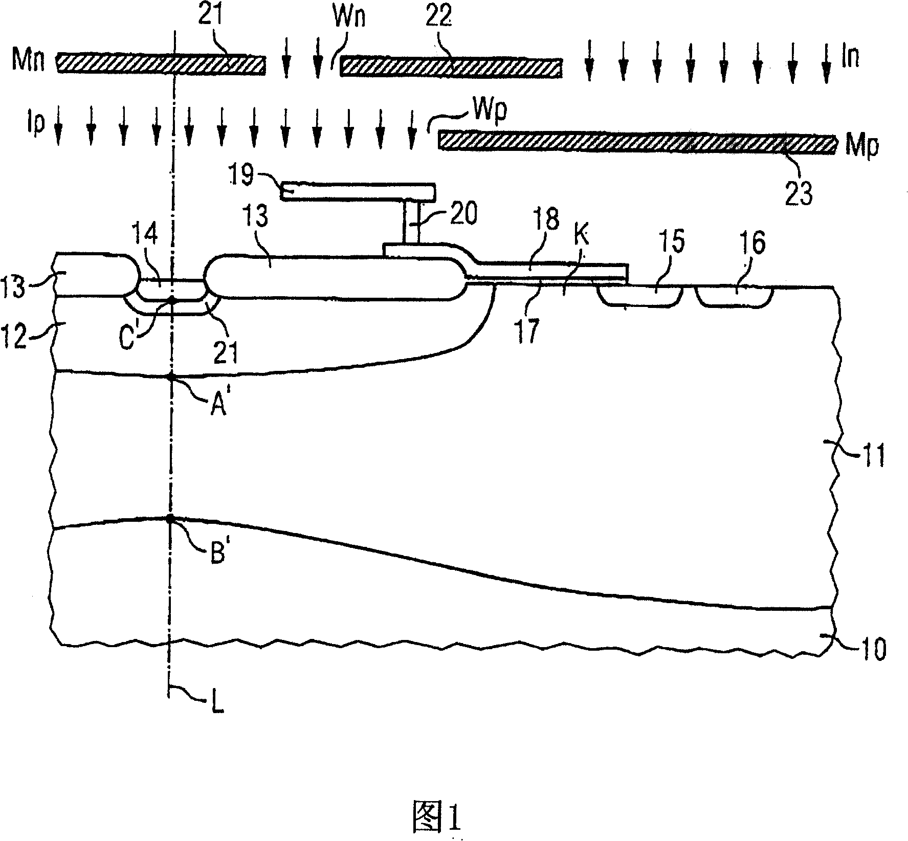
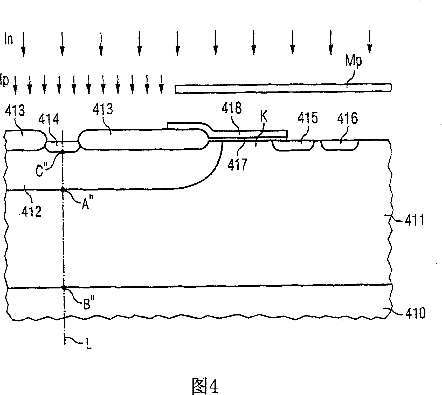
[0021] FIG. 4 shows a refinement of the prior art mentioned at the outset, starting from FIG. 4 for a better overall understanding of the invention. According to FIG. 4 , an n-doped well 411 is arranged on a substrate 410 . A highly doped, p-type conducting region 415 is arranged inside the n-well 411 as a source terminal. Next to it is a highly doped, n-type conductive region 416 which can be used as a ground terminal (Body). A channel region K is connected to the other side of the source region 415 , and a gate electrode 418 , for example composed of polysilicon, is arranged above the channel region K insulated by a gate oxide 417 .
[0022] Arranged in the direction of the drain are field oxide regions 413 which have openings for accommodating a highly doped, p-conducting drain 414 . Below the drain 414 and the field oxide region 413 , a p-doped well 412 is arranged inside the n-doped well 411 , which extends laterally into the channel region. The gate electrode 418 exte...
PUM
 Abstract
Description
Claims
Application Information


