Encapsulation structure of lead rack base ball grid array and its wafer carrier
An array packaging and chip carrier technology, which is applied in the direction of semiconductor devices, semiconductor/solid-state device components, electric solid-state devices, etc. The effect of ball-mounting support strength, preventing mold seal displacement, and improving fixation
- Summary
- Abstract
- Description
- Claims
- Application Information
AI Technical Summary
Problems solved by technology
Method used
Image

Examples
Embodiment Construction
[0071] In order to further explain the technical means and effects adopted by the present invention to achieve the predetermined invention purpose, the following is a concrete implementation of the lead frame base ball grid array packaging structure and its chip carrier according to the present invention in conjunction with the accompanying drawings and preferred embodiments. Mode, structure, feature and effect thereof are as follows in detail.
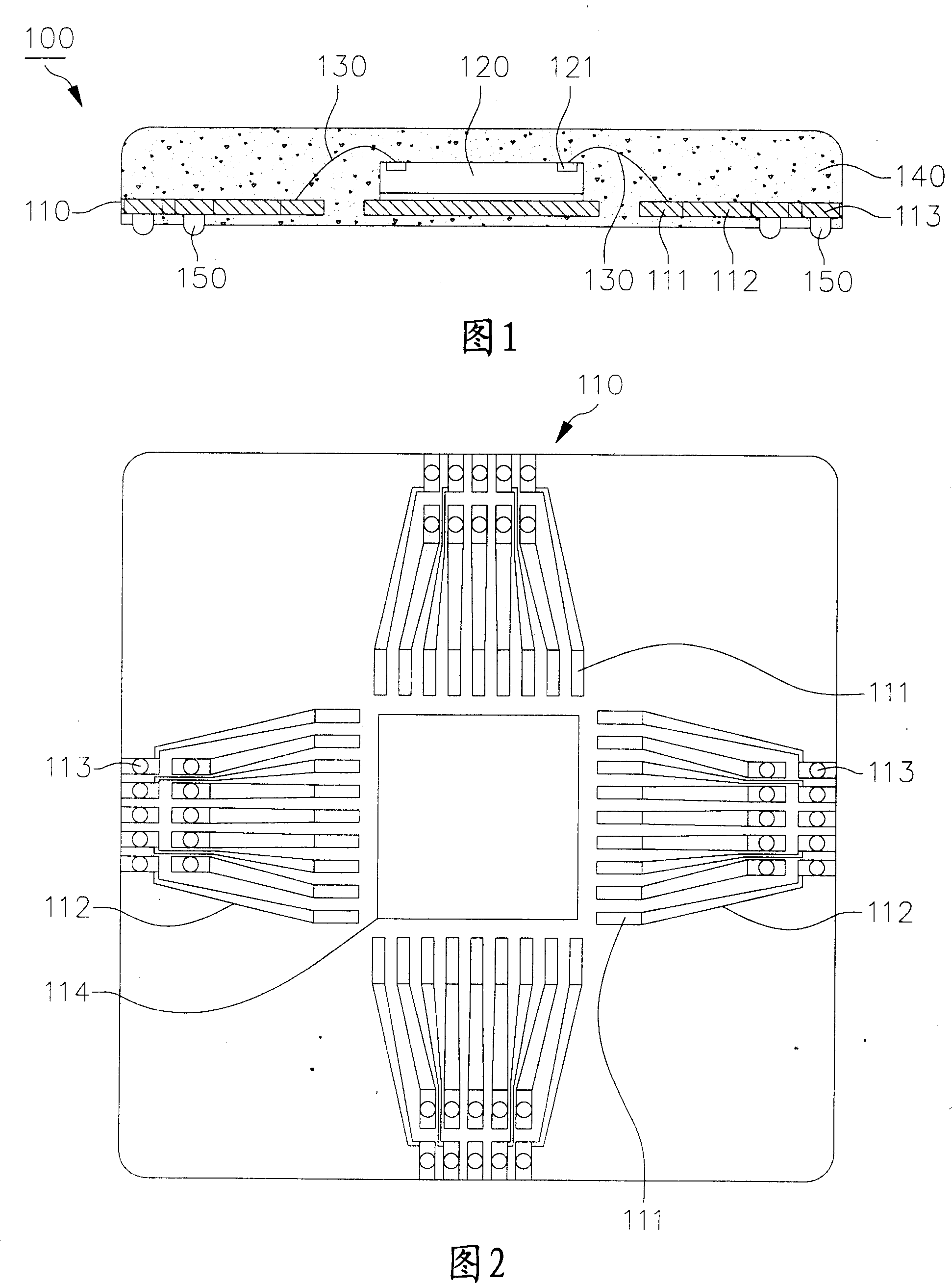
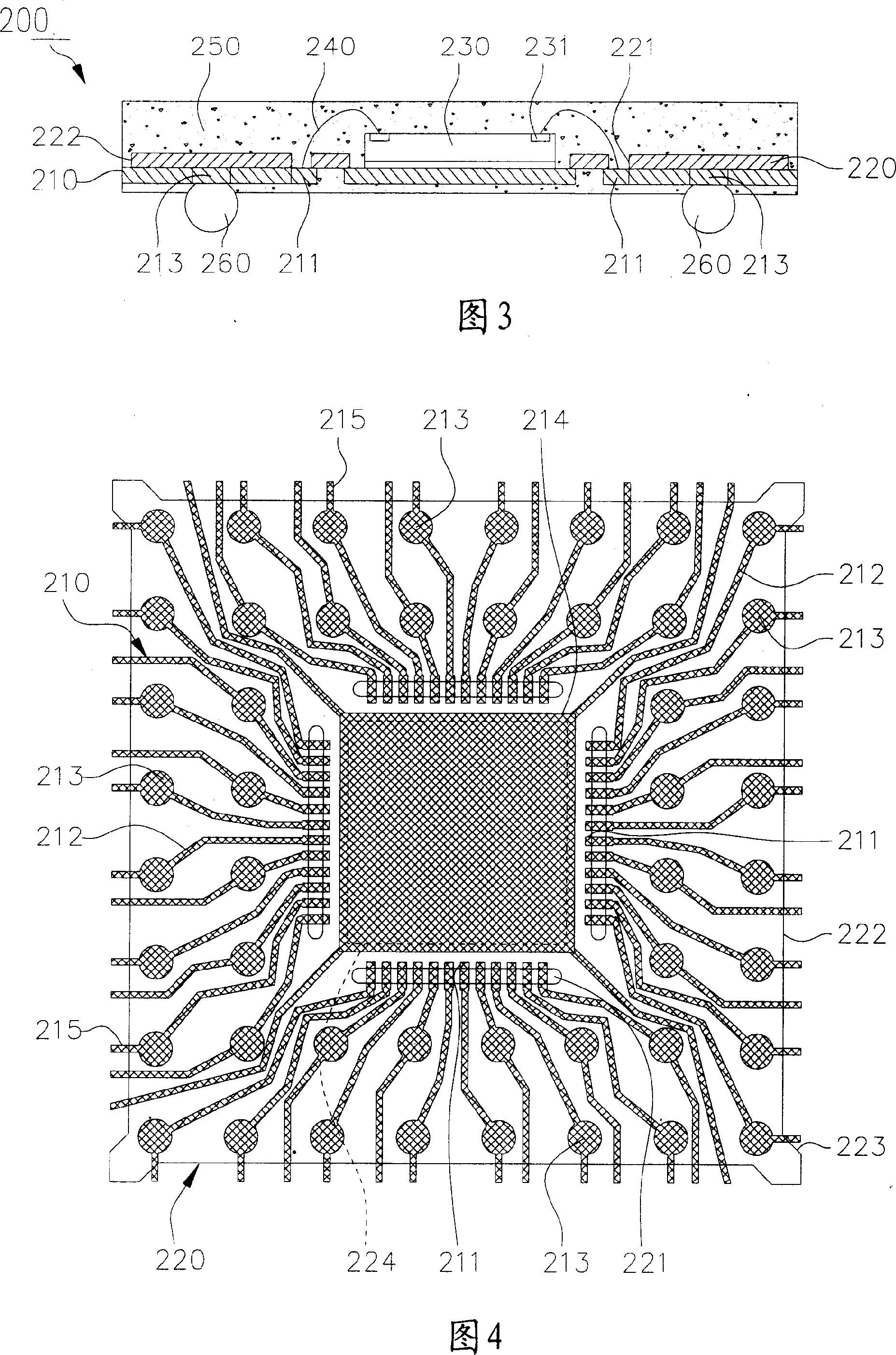
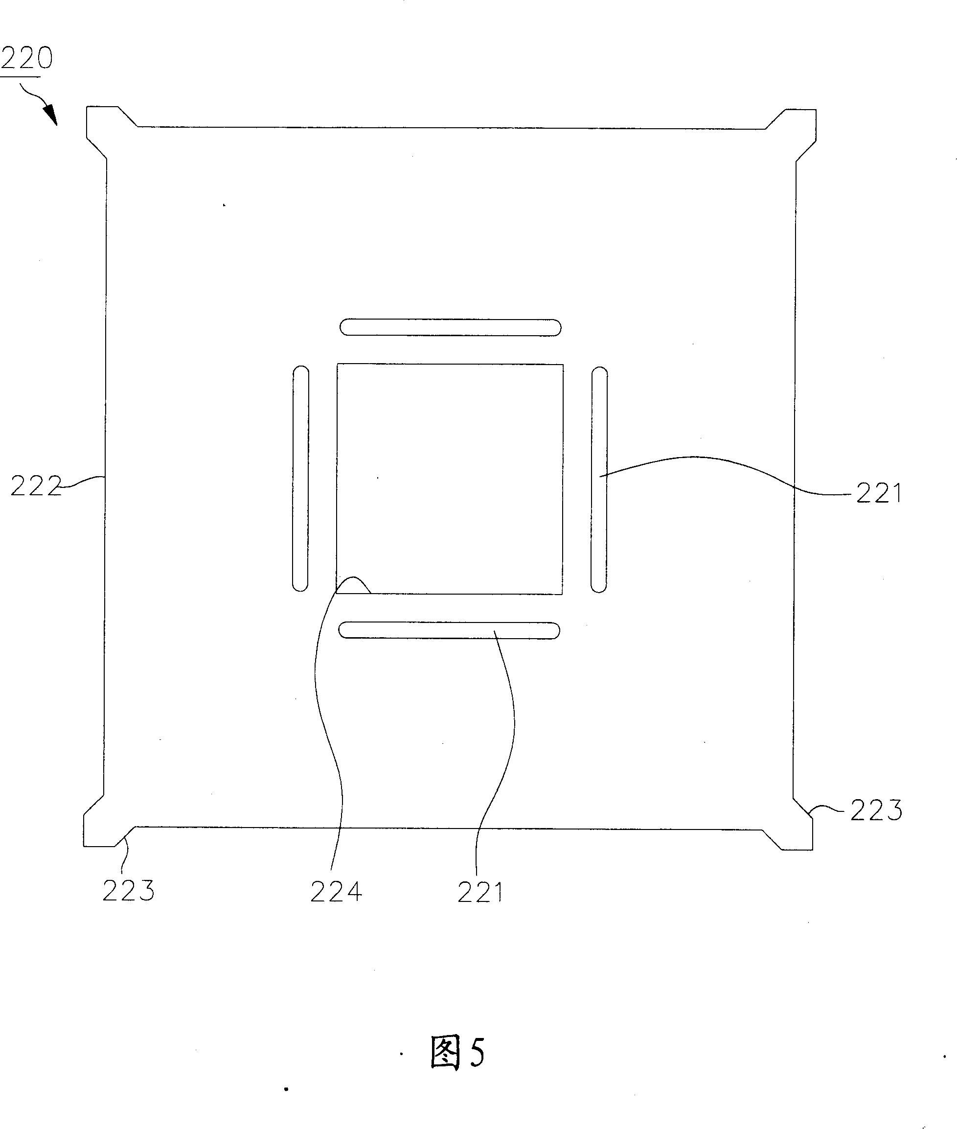
[0072] In a first embodiment of the present invention, a lead frame base ball grid array package structure is disclosed, which is characterized by a lead frame with reconfigurable pins and a hole-type stiffener. Please refer to Figure 3 to Figure 6, Figure 3 is a schematic cross-sectional view of the package structure of the lead frame base ball grid array, Figure 4 is a schematic view of the lead frame and the stiffener of the package structure, and Figure 5 is the stiffener of the package structure Figure 6 is a schematic diagram of...
PUM
 Abstract
Description
Claims
Application Information
 - R&D Engineer
- R&D Manager
- IP Professional
- Industry Leading Data Capabilities
- Powerful AI technology
- Patent DNA Extraction
Browse by: Latest US Patents, China's latest patents, Technical Efficacy Thesaurus, Application Domain, Technology Topic.
© 2024 PatSnap. All rights reserved.Legal|Privacy policy|Modern Slavery Act Transparency Statement|Sitemap